Revision as of 15:29, 27 September 2012
LPCVD (Low Pressure Chemical Vapor Deposition) PolySilicon
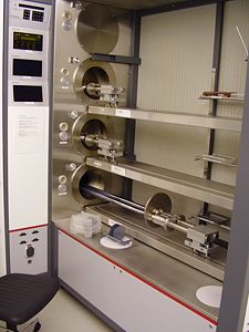
A4 Furnace PolySilicon (situated in cleanroom 2
Danchip has two furnaces for deposition of LPCVD polysilicon: A new 6" furnace (installed in 2011) for deposition of standard polySi, amorphous polySi and boron doped polySi on 4" or 6" wafers and an older 4" furnace (installed in 1995) for deposition of standard polySi, amorphous polySi, boron- and phosphorous doped polySi on 4" wafers. In LabManager the two furnaces are named "Furnace: LPCVD Poly-Si" and "Furnace: LPCVD Poly-Silicon 6inch", respectively. Both furnaces are Tempress horizontal furnaces.
The LPCVD polysilicon deposition is a batch process, where polySi is deposited on a batch of 25 or 50 wafers (6" polySi furnace) or 30 wafers (4" polySi furnace). The polySi has a good step coverage, and especially for standard polySi the film thickness is very uniform over the wafers.
The reactive gas is silane (SiH4). The dopant for boron doped polySi is BCl3 (6" polySi furnace) or B2H6 (4" polySi furnace), and for phosphorous doped polySi the dopant is PH3. For standard polysilion the deposition takes place at a temperature of 620 oC and a pressure of 200-250 mTorr. For amorphous polysilicon the deposition temperatures and thus the deposition rate are lower, and for boron and phosphorous doped polySi the deposition temperature is 600 oC - 620 oC depending on whether you use the 6" or the 4" polySi furnace. For phousphorous doped polySi the deposition rate is approximately ten times lower than for boron doped polySi. More process information about the process parameters can be found in the table below.
To get a training on the furnace please contact training@danchip.dtu.dk.
Information on how to operate the furnaces please read the user manuals which are uploaded to the machine pages in LabManager or consult the Furnace group at Danchip (furnace@danchip.dtu.dk).
Process Knowledge
Please take a look at the process side for deposition of Silicon Nitride using LPCVD:
Deposition of polysilicon using LPCVD
Overview of the performance of the LPCVD polysilicon processes and some process related parameters
| Purpose
|
Deposition of LPCVD polysilicon
|
6" furnace:
- Standard polySi
- Amorphous polySi
- Boron doped polySi (BClFailed to parse (MathML with SVG or PNG fallback (recommended for modern browsers and accessibility tools): Invalid response ("Math extension cannot connect to Restbase.") from server "https://wikimedia.org/api/rest_v1/":): {\displaystyle _3}
dopant)
4" furnace:
- Standard polySi
- Amorphous polySi
- Boron doped polySi (BFailed to parse (MathML with SVG or PNG fallback (recommended for modern browsers and accessibility tools): Invalid response ("Math extension cannot connect to Restbase.") from server "https://wikimedia.org/api/rest_v1/":): {\displaystyle _2}
HFailed to parse (MathML with SVG or PNG fallback (recommended for modern browsers and accessibility tools): Invalid response ("Math extension cannot connect to Restbase.") from server "https://wikimedia.org/api/rest_v1/":): {\displaystyle _6}
dopant)
- Phosphorus doped polySi
|
| Performance
|
Film thickness
|
6" furnace:
- Standard polySi: 0-2000 nm
- Amorphous polySi: 0-1000 nm
- Boron doped polySi: 0-1000 nm
4" furnace:
- Standard polySi: 0-2000 nm
- Amorphous polySi: 0-2000 nm
- Boron doped polySi: 0-2000 nm
- Phosphorus doped polySi: 0-1000 nm
Thicker layers have to be deposited over more runs
|
| Step coverage
|
|
| Film quality
|
- Deposition on both sides of the substrate
- Good uniformity over the wafer
|
| Process parameter range
|
Process Temperature
|
6" furnace:
- Standard polySi: 620 oC
- Amorphous polySi: 560-580 oC
- Boron doped polySi: 600-620 oC
4" furnace:
- Standard polySi: 620 oC
- Amorphous polySi: 560-580 oC
- Boron doped polySi: 620 oC
- Phosphorus doped polySi: 620 oC
The process temperature vary over the furnace tube
|
| Process pressure
|
6" furnace:
4" furnace:
The process pressure depends on the actual process
|
| Gas flows
|
6" furnace:
- SiHFailed to parse (MathML with SVG or PNG fallback (recommended for modern browsers and accessibility tools): Invalid response ("Math extension cannot connect to Restbase.") from server "https://wikimedia.org/api/rest_v1/":): {\displaystyle _4}
: 50-70 sccm
- BClFailed to parse (MathML with SVG or PNG fallback (recommended for modern browsers and accessibility tools): Invalid response ("Math extension cannot connect to Restbase.") from server "https://wikimedia.org/api/rest_v1/":): {\displaystyle _1}
: 1 sccm
4" furnace:
- SiHFailed to parse (MathML with SVG or PNG fallback (recommended for modern browsers and accessibility tools): Invalid response ("Math extension cannot connect to Restbase.") from server "https://wikimedia.org/api/rest_v1/":): {\displaystyle _4}
: 80 sccm
- BFailed to parse (MathML with SVG or PNG fallback (recommended for modern browsers and accessibility tools): Invalid response ("Math extension cannot connect to Restbase.") from server "https://wikimedia.org/api/rest_v1/":): {\displaystyle _2}
HFailed to parse (MathML with SVG or PNG fallback (recommended for modern browsers and accessibility tools): Invalid response ("Math extension cannot connect to Restbase.") from server "https://wikimedia.org/api/rest_v1/":): {\displaystyle _6}
: 7 sccm
- PHFailed to parse (MathML with SVG or PNG fallback (recommended for modern browsers and accessibility tools): Invalid response ("Math extension cannot connect to Restbase.") from server "https://wikimedia.org/api/rest_v1/":): {\displaystyle _1}
: 7 sccm
The silane (SiHFailed to parse (MathML with SVG or PNG fallback (recommended for modern browsers and accessibility tools): Invalid response ("Math extension cannot connect to Restbase.") from server "https://wikimedia.org/api/rest_v1/":): {\displaystyle _4}
) flow depends on the actual process
|
| Substrates
|
Batch size
|
6" furnace:
- 1-25 4" wafers or 6" wafers per run
4" furnace:
Deposition on both sides of the substrate
|
| Substrate materials allowed
|
- Silicon wafers (only clean wafers):
- with layers of silicon oxide or silicon (oxy)nitride (RCA cleaned)
- from furnaces in stack A or B in cleanroom 2
- Quartz wafers (RCA cleaned)
|
