Specific Process Knowledge/Lithography/Mix-and-match
Feedback to this page: click here
Content and illustration by Thomas Pedersen, DTU Nanolab unless otherwise noted.
Mix-and-match lithography is a process in which two lithography processes are combined to produce a pattern in a single resist layer. In this way one can for instance combine the high resolution of E-beam lithography with the high speed of UV lithography. Other combinations using DUV are also possible.
Methods
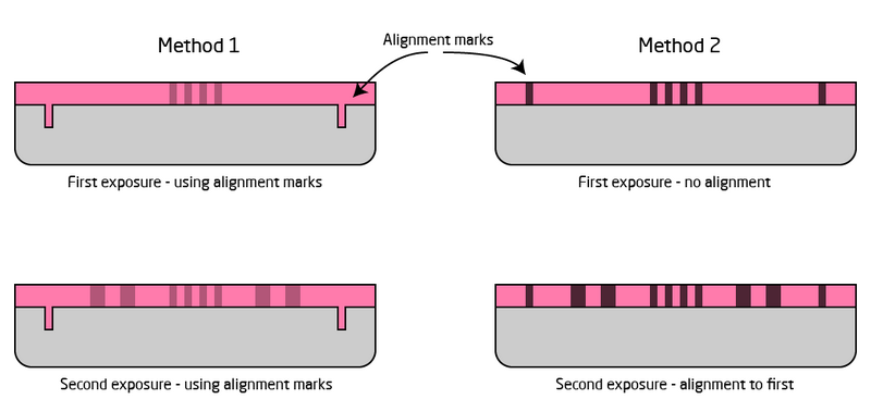
There are two methods for aligning the two patterns to each other, these are illustrated below. In both cases the resist is developed after the second exposure.
- Method 1: In the first method an alignment mark is already present on the substrate and the two exposures are simply both aligned to this and hence they will be aligned to each other.
The second approach relies on the fact that some resist exhibit a slight optical contrast/color change upon exposure and thus it is possible to align a second exposure to the first exposure. This ability is very resist specific.
- Method 2: The second method is thus to perform a first print exposure and subsequently align the second exposure to the slight contrast/color change of the exposed part from the first exposure.
|
|
The two different methods for pattern alignment. |
Alignment accuracy
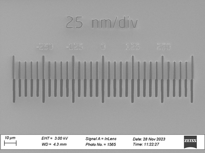
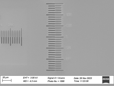
Alignment accuracy is governed by the precision with which one can determine the center of the faint exposed marks and the inherent alignment accuracy of the MLA system. Typical accuracy is found to be +/- 250 nm in both x and y.
 | |  | | 
| ||
|
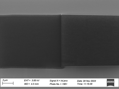
Left and center: Vernier scales for measurement of alignment accuracy. Right: Waveguide where the left side is written by UV and the right side by E-beam. | ||
Mix-and-match resists
nLOF2020
nLOF2020 is found to work as a negative resist for both UV and EBL exposure. After EBL exposure the exposed resist exhibit sufficient contrast change to allow alignment in the MLA systems (specifically verified on MLA2). While it is possible to expose the default 1.5 µm resist layer obtained from the Gamma spin coater system with EBL, in order to obtain a resolution advantage one must dillute the resist to produce a thinner coating as described below.
Test process
Resist used is nLOF2020 diluted in a ratio of 27 grams of resist mixed with 51 grams of PGMEA. The resist is spin coated on Labspin 2 at 2000 RPM for 1 min (1000 RPM/s acceleration). The wafer is then soft baked at 110C for 60 seconds. Resist thickness is 250 nm.
As the resist is UV sensitive exposure to white light in the EBL room is avoided by turning off the light in the room during sample mounting.
A test pattern is exposed with doses from 100 to 600 µC/cm2. After EBL exposure a UV test pattern is exposed on MLA2 utilizing alignment to the exposed resist. After exposure the wafer is developed on Developer: TMAH UV-Lithography using recipe 3005, i.e. a 60 second PEB at 110C and 30 sec single puddle development cycle.
Contrast curve
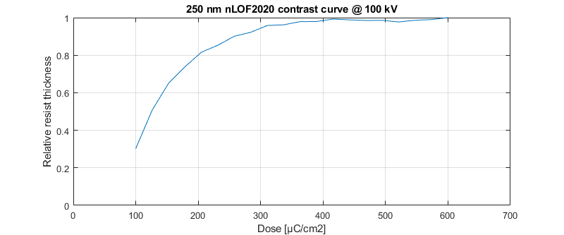
A contrast curve is generated using the parameters described above. The contrast is estimated to be 0.75. The low contrast will limit the possibility of using it for dense and low CD geometry.
|
|
250 nm nLOF2020 contrast curve from exposure at 100 kV on JEOL 9500. |
Example images (250 nm)
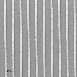
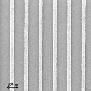
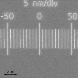
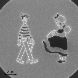
The pattern is written at 6 nA with 10 nm beam pitch, i.e. a fairly high beam pitch in order to accomodate a large dose variation in one sequence. Initial test provides fair definition of lines down to 100 nm, the high line error roughness is most likely from the high beam pitch. A few example images are given below, all from 540 µC/cm2.
 |
 |
 |
|
|
Example images from left to right: 100 nm lines, 150 nm lines, 100 nm vernier scale lines, cartoon figures. Image: Thomas Pedersen. | |||
Example images (1500 nm)
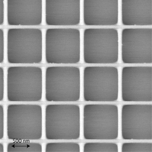
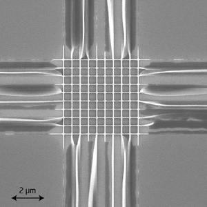
Undiluted nLOF2020 can also be used, in this case a 1500 nm thick resist is exposed at 160 µC/cm2. While it is possible to define lines down to about 100 nm the high aspect ratio will cause free standing lines to collapse as illustrated below.
 |
| ||
|
100 nm lines in 1500 nm thick nLOF2020. | |||