LabAdviser/314/Preparation 314-307/Solid-matter/FIB-lamella
Feedback to this page: click here
(content by Anton Bay Andersen @DTU Nanolab, March 2020)
FIB lamella preparation
The main goal of the lift out process is to extract a small piece of a bulk like sample (typical SEM sample) and attach it to a grid suitable for TEM imaging. The desired sample outcome is a lamella thin enough to be suited for TEM/STEM/EELS/EDX measurements (<100nm is desirable). Throughout this document it is assumed that the operator is an experienced SEM user, always works at eucentric height (the crossover of the ion and electron beam) and has an understanding of the chamber geometry. Furthermore, all settings are material and sample dependent. As a rule of thumb, the harder a material is the more difficult it is to mill with the ion beam. As an example, 20nA is on the low end for milling larger sections of corundum efficiently but 2.8nA is almost too aggressive for gold.
Step: 1,2: Protective Pt deposition
Fig 1: Sketch of electron beam Pt deposition.
Fig 2: Sketch of subsequent platinum deposition.
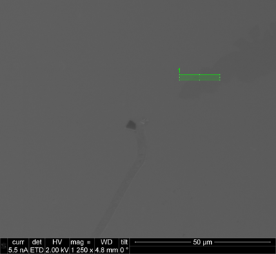
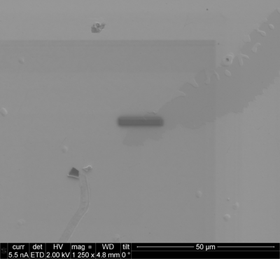
Fig 3: SE images acquired before and after electron beam deposited platinum.
When a suitable region of interest has been located selected by SEM, it is necessary to protect
the surface from damage from the ion beam. A typical deposition scheme is illustrated on
fig 1. The first layer is deposited using the electron beam to minimize surface damage from the subsequent ion beam deposition, imaging and milling. The deposition is done by exposing the sample to a precursor of metal organic gas and scanning the electron beam over the area where deposition is desired. This causes the gas molecules to decompose and parts of the decomposed products deposit on the surface. The electron beam settings used for the deposition are high tension (HT) of 2-5kV with a high current 5.5nA. The deposition thickness listed in the sketch are approximate numbers and are sample dependent. Remember to insert and heat the Pt GIS prior to choose “Pt ebeam structure” for the Pt deposition with the electron beam and the “Pt dep” for deposition with the ion beam. The reason for even having an ion beam deposition afterwards is that the ion beam leaves a much thicker deposition within a reasonable time which protects against the ion beam in the following steps. There is a clear risk of damaging the surface during both depositions. The HT and current used for the ion beam assisted deposition is 30kV and 0.26nA.
Note: A typical stage tilt of 0 degrees and 52 degrees are used for the elctron beam deposition and ion deposition. Your needs may vary depending on sample geometry/requirements. If you wish to use another deposition such as carbon or tungsten you may need to tilt the sample differently.
Step 3,4: Initial rough cut and rough cleaning
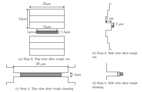
Fig 4: Sketch of the desired rough cut and rough cleaning.
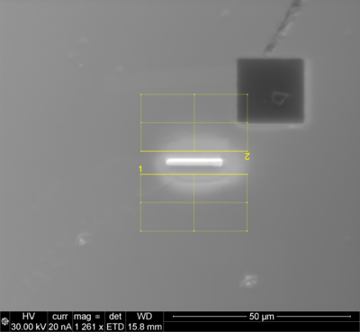
Fig 5: SE images acquired with the ion beam before and after the rough cut.
Fig 6: SE images acquired with the ion beam after the rough cleaning.
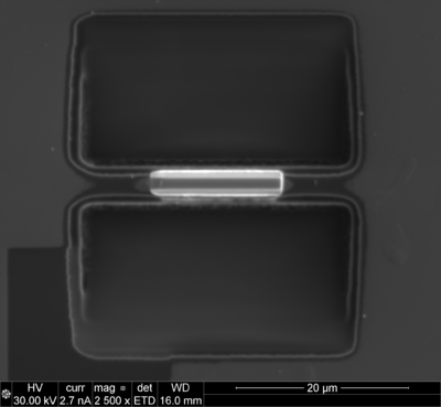
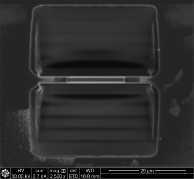
As illustrated in Figure 4-6, the rough cut creates a trench on either side of the region of interest in steps of increasing depth closer to the region of interest. This step milling is to minimize re-deposition of the milled material close to the region of interest. The milling is done by raster scanning the beam in the region where milling is desirable. The depth of the cut is typically chosen to be about 4µm. The deep cut is chosen to achieve sufficient mechanical stability of the final TEM sample, sufficient material at the bottom to mill away in step 5 and sufficient room for milling in step 5 (Milling in very tight quarters leaves heavy re-deposition making the achieved feature deviate heavily from the desired). The trench is positioned a few µm away from the region of interest mainly to accommodate for sample or beam drift while milling. The HT is 30kV and the current is the highest used in the entire process of 9-20nA.The stair step structure is achieved by choosing the “regular cross section” and an application with pure milling such as the “Si” application. Step 4, simply cleans up the sides of the region of interest from re-deposition of milled material and reduces the thickness to that of the region of interest. The same HT of 30kV is used but the current is reduced to 0.9-2.7nA and to achieve a smoother surface the milling is done by scanning a line at a time moving closer to the region of interest/Platinum deposition. This is done using a “cleaning cross section” and a cutting application such as “si”.
Note: If you wish to make cuts perpendicular to the sample surface remember to tilt the stage so the sample correctly. For a flat sample mounted on a flat stub this mean tilting the stage to 52 degrees.
Step 5: Undercut
Fig 7: Illustration of step 5-7.
Fig 8: After undercut from both sides.
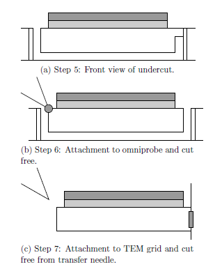
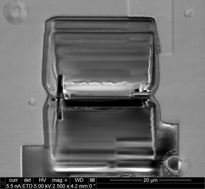
This step cuts a strip away at one side, the entire bottom and half of the other side of the lamella leaving it only supported by a small part in one end. The current used for the cut is 0.44-2.8nA. The usual recommended width of the cuts are 1µm but if redeposition is a problem the width can be increased. As can be seen on figure 8 the undercut must sometimes be done from both sides to ensure
Note: As you wish to through the bottom of the lamellae you need to tilt the sample accordingly. If your lamellae is milled to be perpendicular to the surface it therefore makes sense to set the stage tilt to zero degrees.
Step 6: Attachment to transfer needle and lift out
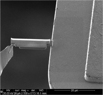
Fig 9: Attachment of the omni probe to a lamellae prior to cutting the lamellae free.
This step attaches the lamella to a very thin needle in one end by a small amount of platinum deposition, using the ion beam and cuts it free at the other end, leaving the lamella hanging on the thin needle. To breaking the lamellae after cutting it free lower the stage first and then begin retracting the omniprobe with the controls.
Note: This step requires the GIS, omni probe inserted. It is recommended that you move the omni probe in position manually, that is with the controls, as the “insert omniprobe” overshoots a large amount. When you press insert omniprobe should appear at the lower left part of the ion beam view at the lowest magnification.
Step 7: Attachment TEM grid
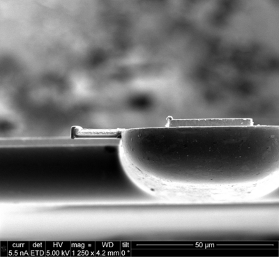
Fig 10: Attachment of the omniprobe to the omniprobe grid.
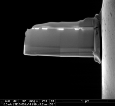
This step transfers the needle to the TEM grid. The lamella is brought close to the TEM copper grid by moving the omniprobe, a thin platinum strap is deposited using the ion beam on the grid and the platinum attaching the lamella to the needle is cut away. Please do not cut into the omniprobe during this step.
Step 8: Final thinning with Ga beam
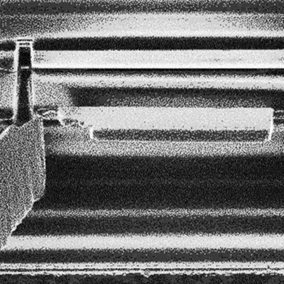
Fig 11: Viewing directions during thinning. Left ion beam, right electron beam.
After step 7 the result is a lamella attached to a TEM grid with a thickness far too high for TEM investigations. The sample is then successively thinned with the ion beam from the view seen in figure 10. Again the cleaning cross section should be used. The current should be lowered stepwise through this process. The indicator used to judge the thickness of the sample is the protective platinum layer since thinning tends to leave a wedge shape with the thinnest part being the protective platinum. Depending on how thin the sample is desired to be the thinning is stopped when the platinum is close to disappearing or when it has been removed in some regions leaving very thin areas next to these. The sample might still be thicker than desired after this step if the thinning is stopped before the protective platinum is removed from some regions, depending on the composition. If this is the case, or if the side wall damage is undesireble, low kV cleaning can be performed by simply lowering the acceleration voltage of the ion gun and scanning the beam over the sample, after tilting slightly. Note that the CDEM detector is more useful than the ETD detector in this case. Typical values are 5 degrees over and undertilt, 1-5kV, 26pA and a milling time on either side of 10min.
Note: Milling like described above makes a wedge shaped sample. This increases mechanical stability while still making an extremely thin sample at the surface. If a flat sample is desired you can compensate by tilting the sample. The amount of tilt depends on material, acceleration voltage and current, so a bit of experimenting is required.


