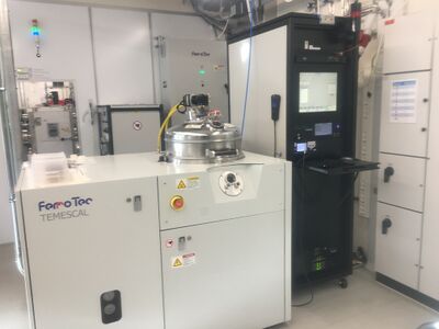
Specific Process Knowledge/Thin film deposition/10-pocket e-beam evaporator
Feedback to this page: click here
This page is written by DTU Nanolab staff
This page is under construction
E-Beam Evaporator (10-pockets)

The 10-pocket e-beam evaporator is a system for depositing materials by electron-beam evaporation. In e-beam evaporation, the deposition is line-of-sight from the source, which means it will coat only the surface of the sample facing directly towards the source. This makes it very useful for example for lift-off. This particular machine was purchased by Nanolab in 2023. It is made by Temescal, a division of FerroTec, and is very similar to the other e-beam evaporator we have from the same manufacturer, bought in 2018, which we call E-beam Evaporator (Temescal) in the LabManager system.
In both Temescal e-beam evaporators, wafers are loaded into the top of the chamber, called the product chamber, which acts as a loadlock as it can be separated from the rest of the chamber by a large gate valve. Deposition will happen on all samples that are loaded together. You can load up to four 6" wafers or three 8" wafers for deposition on surfaces facing the evaporation source, or on up to one 6" wafer for tilted deposition. By using sample holder inserts, you can deposit metals on samples of different sizes and shapes. Only one metal can be deposited at a time, but you can deposit many layers of different metals one after the other. The system contains 6 metals at a time and the metals are exchanged based on user requests, so please request the metals you wish well in advance.
Some special features of the 10-pocket system compared to the other Temescal e-beam evaporator is that is can be used with sample heating up to 250 °C and with a low oxygen flow. We allow deposition of silicon and of thin layers of oxides in this machine - apart from the metal oxides, this includes silica and alumina. However, you need specific training to use these options.
The user manual, user APV, and contact information can be found in LabManager:
E Beam Evaporator (10-pockets) in LabManager
Training videos may be found here:
Process information
- Acceptance Test. Describes thickness uniformity tests, side wall deposition tests, sheet resistance tests and tests of the ion source for substrate cleaning.
Materials for e-beam evaporation
These materials are available in the 10-pocket e-beam evaporator:
- Aluminium (Al)
- Chromium (Cr)
- Copper (Cu)
- Germanium (Ge)
- Gold (Au)
- Nickel (Ni)
- Platinum (Pt)
- Silver (Ag)
- Titanium (Ti)
Plus some MORE
Thickness measurement, deposition rate and process control
Read about how the machine measures the thickness of the growing film using a quartz crystal monitor, how accurately you can control the rate/thickness, and other useful information about e-beam deposition here: Thickness, rate, process control.
Particulates in the films
Read about optimizing film quality including how to minimize the number of particulates in Au films in the Temescal.
| Purpose | Deposition of metals |
|
|---|---|---|
| Performance | Film thickness |
|
| Deposition rate |
| |
| Thickness uniformity |
| |
| Thickness accuracy |
| |
| Process parameter range | Process Temperature |
Higher for refractive metals that require a lot of heat to evaporate, see above. |
| Process pressure |
| |
| Source-substrate distance |
| |
| Substrates | Batch size |
|
| Substrate material allowed |
| |
| Material allowed on the substrate |
|
* For thicknesses above x nm please request permission so we can ensure that enough material will be present.
** Defined as the ratio of the standard deviation to the average of the measurement made using the DektakXT. For further details see the acceptance test.

