LabAdviser/Technology Research/Presentation Form/Process flow form
| Step | Description | LabAdviser link | Image showing the step | |
|---|---|---|---|---|
| 1.1 | Si wafer | Start with a 100 mm Si<100> wafer that is single side polished and p doped with boron. This will be the absorber in the final solar cell. | Wafer information, types of avaliable wafers are listed. | |
| 1.2 | RCA clean | The wafer has to be RCA cleaned, before entering an oxidation furnace. | RCA cleaning, the different steps in the cleaning procedure are described. | |
| 1.3 | SiO2 dry oxidation | Grow a dry thermal oxide layer in the Boron Drive-in furnace (A1). The oxide layer will be patterned later on to define n-doped areas ("electron membrane".) | Boron Drive-in furnace, info about performance and process parameter range. |  |
2 Lithography and oxide etch
| Step | Description | LabAdviser link | Image showing the step | |
|---|---|---|---|---|
| 2.1 | HMDS surface treatment | To ensure the resist sticks to the surface, the wafer is HMDS treated before resist spinning. | HMDS oven | |
| 2.2 | Spin resist on wafer backside | The backside of the wafer needs to be protected, to prevent the SiO2 from being etched in the first etch step (section 3). | Resist spinners. Information about what resists that can be used with the spinners. |  |
| 2.3 | Spin resist on wafer frontside | The frontside of the wafer is covered with a resist layer. | Information about resist processing, positive and reversed lithography processes. |  |
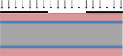
| 2.4 | Expose photoresist in aligner | The resist layer on the wafer frontside is exposed in the aligner, with a dark field mask. Align the mask to wafer flat, and use hard contact. | Aligner-6inch - EVG620. Here you can see a comparison between different aligners. |  |
| 2.5 | Develop photoresist | In the development step the exposed resist is removed, so that a resist pattern is formed on the surface. | Development, standard development times are listed. |  |
| 2.6 | Optical microscope inspection | Check the results of the exposure and development with an optical microscope by inspecting that the pattern and alignment marks are clearly visible. Right image: top view of alignment marks. The alignment marks will be used to align the wafer to the mask in next lithography step (section 5). | The different optical microscopes and their features are listed. |  |

