Specific Process Knowledge/Lithography/EBeamLithography
Feedback to this page: click here
The JEOL JBX-9500 electron beam lithography system is a spot electron beam type lithography system designed for writing patterns with dimensions from nanometers to sub-micrometers. The minimum electron beam is around 5 nm, the maximum writitng field without stitching is 1 mm x 1 mm.
The machine is located in a class 10 cleanroom (E-2) with tight temperature and moisture control. The room must only be entered when the machines or equipment inside the room is intended to be used.
You can read more about electron beam writing in this book published by SPIE.
The user manual, technical information and contact information can be found in LabManager:
Performance of the e-beam writer
| Purpose | pattern an electron sensitive resist | Mainly for pattering structures with minimum feature size between 12 nm - 1 µm |
|---|---|---|
| Performance | Resolution |
|
| Maximum writing area without stitching |
| |
| Process parameter range | E-beam voltage |
|
| Scanning speed |
| |
| Min. electron beam size |
| |
| Min. step size |
| |
| Beam current range |
| |
| Dose range |
| |
| Samples | Batch size |
Wafer cassettes:
|
| Substrate material allowed |
|
Getting started
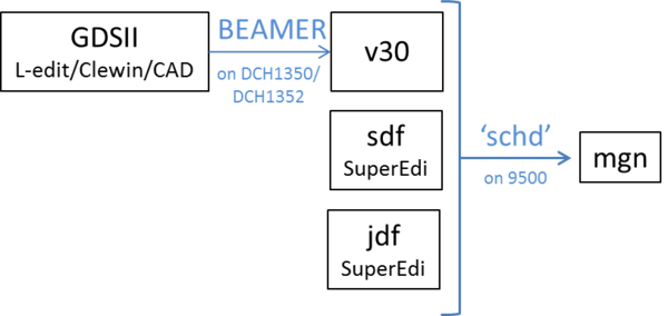
To request for an e-beam training session, contact e-beam@danchip.dtu.dk; a DTU Danchip personnel will hereafter provide a time slot. Users require at least 4 training sessions before being allowed full acccess to the machine. The first training will focus on file preparation and compilation alone.
Before you request for a training on the machine
- It is crucial to have your pattern ready in GDSII format. Check your GDS-file by importing it in e.g. CleWin or L-edit. In order to reach the files from the computers inside the cleanroom it is recommended to either dropbox them or send them per email to yourself.
- Create sdf and jdf-files:
- Assist a fully trained colleague of yours when she or he e-beam writes, gather as much knowledge about your e-beam run, i.e. which e-beam current, aperture and dose to use, which shot pitch (e.g. SHOT A,10).
- Study the logbook for the e-beam writer: sheet 1 gives you an overview of which condition files (currents and apertures) have been in use recently by which user on which type of resist. On sheet 2 in this logbook you can find a writing time estimation program.
- Study all 3 manuals for the machine, they can be found here
General Rules
For safety reasons, even fully trained users are only authorized to mount substrates into the e-beam cassettes, but not authorized to load the cassettes into the autoloader.
There are two daily loading sessions where cassettes will be loaded into the autoloader by trained DTU Danchip personel:
- 10:00
- 13:30
To use the e-beam writer, book the machine via LabManager, note the number and type of substrate as well as the condition file to be used in the 'Public Comment:' field in LabManager. Mount your substrate in the cassette (and pre-align if necessary) before the loading session preceding your booking, and show up at the time your cassette is loaded.
After your exposure, fully trained users can unload their cassettes from the autoloader, unmount their substrates and re-load an empty cassette into the autoloader. If you are prohibited to unmount your substrates before another user requires the cassette, you must accept that either the next user or DTU Danchip personel unmount your substrates.
Manuals
There are 3 manuals for the e-beam writer:
- A user manual describing the standard procedure when e-beam writing
- A jdf-, and sdf-file manual describing how to prepare sdf-, and jdf-files (found under 'Technical Documents')
- A BEAMER manual describing how to convert your pattern file (GDSII-format) to v30-format (found under 'Technical Documents')
E-beam resists and Process Flows
The table describes the e-beam resist used in the cleanroom for standard e-beam exposure. Some of resists are not provided by DTU Danchip and some are not yet approved for common use in the cleanroom and are currently being tested. If you wish to test some of these resists or other resists, please contact Lithography.
Standard DTU Danchip resists purchased and tested by DTU Danchip:
| Resist | Polarity | Manufacturer | Comments | Technical reports | Spinner | Developer | Rinse | Remover | Process flows (in docx-format) |
| CSAR | Positive | AllResist | Standard positive resist, very similar to ZEP520. | Allresist_CSAR62_English.pdf,, CSAR_62_Abstract_Allresist.pdf | Manual Spinner 1 (Laurell), Spin Coater Labspin | XAR-600-546, XAR-600-548, N50, MIBK:IPA | IPA | AR-600-71, 1165 Remover | Process Flow CSAR.docx |
| ZEP520A | Positive | ZEON | Positive resist | ZEP520A.pdf, ZEP520A spin curves on SSE Spinner | SSE, Manual Spinner 1 (Laurell), Spin Coater Labspin | ZED-N50/Hexyl Acetate,n-amyl acetate, oxylene. JJAP-51-06FC05.pdf, JVB001037.pdf | IPA | acetone/1165 | Process_Flow_ZEP.docx, Process_Flow_ZEP_with_Al.docx
|
| ZEP7000 | Positive | ZEON | Not approved and not yet purchased. Low dose to clear, can be used for trilayer (PEC-free) resist-stack. Please contact Lithography for information. | ZEP7000.pdf | Manual Spinner 1 (Laurell), Spin Coater Labspin | ZED-500/Hexyl Acetate,n-amyl acetate, oxylene. | IPA | acetone/1165 | Trilayer stack: Process_Flow_Trilayer_Ebeam_Resist.docx
|
| Copolymer AR-P 617 | Positive | AllResist | Approved, not tested yet. Used for trilayer (PEC-free) resist-stack or double-layer lift-off resist stack. Please contact Lithography for information. | AR_P617.pdf | Manual Spinner 1 (Laurell), Spin Coater Labspin | AR600-55, MIBK:IPA | acetone/1165 | Trilayer stack: Process_Flow_Trilayer_Ebeam_Resist.docx | |
| mr EBL 6000.1 | Positive | MicroResist | Standard negative resist | mrEBL6000 processing Guidelines.pdf | Manual Spinner 1 (Laurell), Spin Coater Labspin | mr DEV | IPA | mr REM | Process_Flow_mrEBL6000.docx
|
| HSQ (XR-1541) | Negative | DOW Corning | Approved. Standard negative resist, mainly for III-V materials | Spin Coater Labspin | TMAH, AZ400K:H2O | H2O |
| ||
| ma-N 2403 | Negative | Micro Resist | Approved. Standard negative resist. | Spin Coater Labspin | Ma-D333, TMAH, MIF726 | H2O | acteone/O2 plasma | ||
| AR-N 7520 | Negative | AllResist | Both e-beam, DUV and UV-sensitive resist. Currently being tested, contact Peixiong Shi for information. | AR-N7500-7520.pdf | Manual Spinner 1 (Laurell), Spin Coater Labspin | AR 300-47, TMAH |
|
Non-standard DTU Danchip resists not purchased by DTU Danchip:
| Resist | Polarity | Manufacturer | Comments | Technical reports | Spinner | Developer | Rinse | Remover | Process flows (in docx-format) |
| PMMA | Positive | We have various types of PMMA in the cleanroom, none are provided by DTU Danchip. Please contact Lithography for information. | Manual Spinner 1 (Laurell), Spin Coater Labspin | MIBK:IPA (1:3), IPA:H2O | IPA | acetone/1165/Pirahna |
Alignment of exposure to existing pattern on wafer
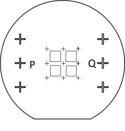
If you need to align an exposure to an existing pattern on a wafer you need wafer marks (or global marks) to align your exposure to. If you are exposing chips (i.e. many small GDS-files you repeat in a matrix), chip marks is recommended to align every chip.
Please note that manual alignment (using the SEM) is not allowed. You should use semi-automatic alignment only. In rare cases where semi-automatic alignment is impossible, you should remove the resist around the wafer marks before loading the wafer/chip into the machine.
1 Material: Global marks or chip marks should be clearly visible in a 100keV SEM, i.e. preferably defined by Ti/Au or another 'heavy' metal, alternatively the wafer marks should be etched. Shallow etched (even 200 nm etched profiles) global marks or global marks defined by a light metal as Al can be hard to locate manually as well as automatically.
2 Design:
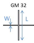
- Global marks: You need at least two wafer marks, a P mark and a Q mark. It is recommended to have many P and Q marks available on the wafer to choose from. The x-coordinate of the P mark should be smaller than the x-coordinate of the Q mark. The global marks should either be crosses or L-shaped, they should be as narrow as possible and 500 - 1000 microns in length. If the wafer contains a number of identical marks, the marks should be marked in order to identify the 'right' alignment mark (the scan width of the SEM is 1 mm x 1 mm). Text around the wafer mark is NOT recommended. Wafer marks formed as crosses with lengths of 1000 microns and 3-5 microns in width are recommended.
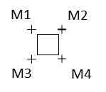
- Chip marks: Prepare 1 or 4 chip marks on every chip. The chip marks can be smaller than global marks, as only very fine alignment is performed with chip marks. The chip marks should either be crosses or L-shaped and text around the marks is NOT recommended.
Proximity Error Correction
Even though the electron beam diameter is below 5 nm, the feature and pitch resolution in resist is limited by the forward and backward scattering of the electrons. The forward scattering depends on the electron acceleration voltage, the resist material and thickness. The backward scattering depends on the electron acceleration voltage and the substrate material [1], [2].
As the travel distance of backscattered electrons is fairly large, e-beam patterned structures will be influenced by adjacent e-beam patterned structures, i.e. a proximity effect. These proximity effects can be avoided either by simulating a proximity error correction (PEC) in BEAMER or by using the right stack of e-beam resist.
Proximity Error Correction (PEC) in BEAMER
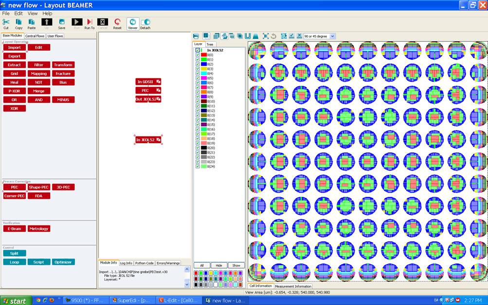
BEAMER is endowed with a software that corrects for proximity errors in the e-beam exposure. You can read more about this function in the BEAMER manual in LabManager under Technical Documents here and in the BEAMER presentation here BEAMERPresentation.pdf.
The proximity error correction require a forward and a backward range parameter, alfa and beta, and a ratio of backscattered energy to the forward scattered energy, eta. As alfa depends on the electron acceleration voltage, which is constant at 100kV, alfa is in BEAMER fixed to 0.007. Help to find beta and eta can be found here.
Alternatively, a point-spread function can be used in BEAMER to calculate the optimised dose-variation.
Trilayer resist stack
As an alternative to PEC, a trilayer reists stack with a thin layer of thermally evaporated Ge can be used [3]. This reists stack has not yet been tested at DTU Danchip. A process flow for this procedure can be found here Process_Flow_Trilayer_Ebeam_Resist.docx, but please contact Lithography before use.
Charging of non-conductive substrates
All substrates are grounded to the cassette when properly loaded. In a non-conducting substrate, the accumulation of charges in the substrates will however destroy the e-beam patterning. To avoid this, a charge dissipating layer is added on top of the e-beam resist; this will provide a conducting layer for the electrons to escape, while high-energy electrons will pass through the layer to expose the resist.
If you wish to investigate the charge dissipation using other methods than below, please contact Lithography.
ESPACER
Espacer is a chemical that works as a discharging layer; it is spun onto the wafer on top of the resist and easily rinsed off the wafer after e-beam exposure. Visit this page for more information: Espacer
Aluminum coating
At DTU Danchip, we recommend to use a thin (20 nm) layer of thermally evaporated aluminum on top of the e-beam resist. Preferably, the thickness of Al and the e-beam dose should be optimised to the features you wish to e-beam pattern [4]. A good starting point is 20 nm Al; from here dose and development can be optimised to reach the resolution and feature size required.
The process flow for a standard e-beam exposure on ZEP520 with Al on top can be found here Process_Flow_ZEP_with_Al.docx.


