Specific Process Knowledge/Thermal Process/C3 Anneal-bond furnace
Feedback to this page: click here
Anneal-bond furnace (C3)

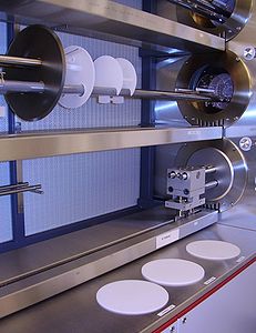
The Anneal-bond furnace (C3) is a Tempress horizontal furnace for oxidation and annealing of new and processed (e.g. bonded) silicon wafers. O2) is used as an oxidant for dry oxidation, and for wet oxidation water vapour is being generated by a bubbler.
This furnace is the third tube in the furnace C-stack positioned in cleanroom B-1.
In this furnace it is allowed oxidize and anneal new wafers without doing an RCA clean first. Also silicon wafers from PECVD4 and wafers without any metal coming from PECVD3 and bonded wafers comming directly from the Wafer Bonder 02 (assuming they were clean and not have been exposed to any metal when entering wafer bonder) can be processed in the furnace without an RCA cleaning. Check the cross contamination information in LabManager before you use the furnace.
The user manual, technical information and contact information can be found in LabManager:
Process knowledge
| Purpose |
|
Oxidation:
|
|---|---|---|
| Performance | Film thickness |
|
| Process parameter range | Process temperature |
|
| Process pressure |
| |
| Gas flows |
| |
| Substrates | Batch size |
|
| Substrate materials allowed |
|
