Specific Process Knowledge/Etch/DRIE-Pegasus: Difference between revisions
No edit summary |
|||
| Line 141: | Line 141: | ||
== Process applications == | == Process applications == | ||
[[Media:Aerospace.pdf |MEMS in Aerospace]]. | [[Media:Aerospace.pdf |MEMS in Aerospace]]. | ||
Revision as of 12:41, 26 November 2012
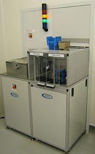
The DRIE Pegasus at Danchip

The Bosch process
The DRIE Pegasus is a state-of-art silicon dry etcher that offers outstanding performance in terms of etch rate, uniformity etc. It uses the so-called Bosch process to achieve excellent control of the etched features. Click here for more fundamental information of the system.
User manuals etc.
The user manual, quality control procedure and the results may all be found on the DRIE-Pegasus LabManager page.
Important information
In August 2011 we introduced a new set of rules regarding the loading of wafers. In you were trained prior to this, you can find more information here.
Acceptance test
The instrument was opened for users in April 2010 when the acceptance test was signed. This was based on the performance of five standard recipes (A, B, C, D and SOI) that are further examined below. The acceptance test report is found here.
Process information
Process notation
Describing a process recipe on the Pegasus may sometimes be difficult because of the great flexibility of the instrument. A compact and precise notation is therefore required for the recipes. Click here to find a short description of the official SPTS notation.
Standard recipes
The standard processes: Processes A, B, C, D and SOI
The instrument was accepted on the basis of the performance of 5 processes. These standard processes are described below.
| Process name | Type | Purpose | Conditions during original runs | Best usage | |||
|---|---|---|---|---|---|---|---|
| Feature | Mask material | Etch load | Comments | ||||
| Process A | Bosch | Fast etch | 80 µm trench | Photo resist | 12-13 % on 6" wafer | ||
| Process B | Bosch | Fast etch | 30 µm diameter via | Photo resist | 12-13 % on 6" wafer | ||
Process A
Process A is labelled Large trench (80μm wide) 150μm depth. In the acceptance test the process was run on a 150 mm SPTS wafer with 12-13 % etch load.
Process A: Recipe, specifications and results
Process B
Process A is labelled Via (30μm diameter) 100μm depth. In the acceptance test the process was run on a 150 mm SPTS wafer with 12-13 % etch load.
Process B: Recipe, specifications and results
Process C
Process A is labelled Nano silicon etch. In the acceptance test the process was run on a 100 mm Danchip wafer with a test pattern of a series of lines and dots with sizes ranging from 30 nm to 300 nm. The etch load was extremely high, approaching 100 %.
Process C: Recipe, specifications and results
Process D
Process D is labelled Micro stamp etch.
In the acceptance test the process was run on a 100 mm wafer with 50 % etch load.
Process D: Recipe, specifications and results
SOI etch
The SOI etch uses the Low frequency (LF) platen generator to minimize the notching at buried stop layers such as the BOX layer in a SOI wafer.
SOI etch: Recipe, specifications and results
Other processes
Nanoetching
Wafer thinning
Sloped sidewalls
For injection molding purposes
Processing challenges
Bonded wafers
User manuals
- The Danchip user manual from LabManager is found >Here<.
- The user manual provided by SPTS can be found here >HERE<
Hardware information
Hardware Information - Overview.
Hardware Information - Detailed.
The Advantages the Pegasus has over existing Si etchers.
Robot Handling System Information .
Process applications
Further info:
