Specific Process Knowledge/Lithography/EBeamLithography/FirstEBL: Difference between revisions
| Line 129: | Line 129: | ||
Beamer uses a node based system where nodes are applied in sequence. In this example there is only an import and an export node. | Beamer uses a node based system where nodes are applied in sequence. In this example there is only an import and an export node. | ||
|} | |} | ||
Each node has several options and these can be changed by double clicking the node. For the export node we will need to choose the correct machine in "Machine Type", the DTU Nanolab system is "JBX-9500FS (100kV)". On the advanced tab we will choose "Floating" field ordering and "Center to Field". This will ensure that our features/pattern will be written in the center of the writing field. The setup will look like the parameters below. | Each node has several options and these can be changed by double clicking the node. For the export node we will need to choose the correct machine in "Machine Type", the DTU Nanolab system is "JBX-9500FS (100kV)". On the advanced tab we will choose "Floating" field ordering and "Center to Field". This will ensure that our features/pattern will be written in the center of the writing field. The setup will look like the parameters below. | ||
{| style="border: none; border-spacing: 0; margin: 1em auto; text-align: center;" | |||
[[ | |- | ||
| [[image:BEAMER_setup.png|800px]] | |||
|- | |||
| colspan="1" style="text-align:center;| | |||
Beamer uses a node based system where nodes are applied in sequence. In this example there is only an import and an export node. | |||
|} | |||
Revision as of 22:07, 17 February 2023
My First JEOL 9500 Exposure Guide
The JEOL 9500 E-beam writer offers world class performance, this however comes at a price of a fairly steep learning curve. This page is specifically intended to guide new users through their very first exposure on the system. In this guide we will set up a simple wafer/chip exposure using a single beam current and without pattern alignment. The complexity of this job is kept at a very low level and we encourage new users to make sure their first job (first training session) matches this complexity level. More complex jobs can be run when a user is more familiar with the system.
Example job
The example provided here demonstrates one way to set up a dose test of a particular pattern on a blank 4" silicon wafer. Dose testing is often necessary to obtain the desired critical dimension and it is vital to be able to set up such a job in an efficient manner. In this example we set up the dose variation/modulation by manually writing a short modulation table. For more complex dose tests or dose test of proximity corrected patterns one should consider using the Chipplace module found in Beamer.
The pattern used in this example is a DTU logo.
JEOL 9500 example workflow
The workflow of our example JEOL 9500 job is summarized below and explained in detail in the subsequent sections. In order to optimize usage of the system steps 1 through 3 must all be done ahead of the booked session on the 9500 system.
- Substrate preparation - resist coating
- Pattern preparation - export to JEOL52 V3.0 (V30) format
- Job preparation
- Jobdeck file (JDF) and schedule file (SDF) preparation
- Job file compilation
- Job verification
- Exposure session
- Sample loading
- System calibration
- Exposure
- Cassette and sample unloading
- Development
In the following we will look at each step in more detail and show step by step how to make a wafer/chip exposure.
Resist coating
DTU Nanolab offers a few different standard resist as given in the table below. Typically layers of 50-500 nm are applied. The Gamma UV & E-beam coater has predefined recipes for various thickness of CSAR resist. For other thickness or other resist the more manual Lab Spin 2 or 3 coasters can be used.
| DTU Nanolab supplied standard EBL resists and process guides | ||||||||||
|---|---|---|---|---|---|---|---|---|---|---|
| Resist | Polarity | Manufacturer | Technical reports | Spin Coater | Polynomial | Thinner | Developer | Rinse | Remover | Process flows (in docx-format) |
| CSAR AR-P 6200 | Positive | AllResist | AR-P 6200 info | Spin Coater: Gamma E-beam and UV or Spin Coater: LabSpin 02/03 | a = 7252, b = -0.454 | Anisole |
|
IPA |
|
CSAR CSAR with Al LOR5A with CSAR |
| Medusa AR-N 8200 | Negative | AllResist | AR-N 8200 info | Spin Coater: LabSpin 02/03 | a = ?, b = ? | AR 600-07 | AR 300-47:DIW (1:1) | DIW | BOE | |
| AR-N 7500 | Negative | AllResist | AR-N 7500 info | Spin Coater: LabSpin 02/03 | a = 17126, b = -0.435 | PGMEA |
|
DIW |
|
|
Resist thickness as function of spin speed on Lab Spin 2/3 can be estimated from the parameters above as y = axb, where y is resist thickness in nm and x is spin speed in RPM.
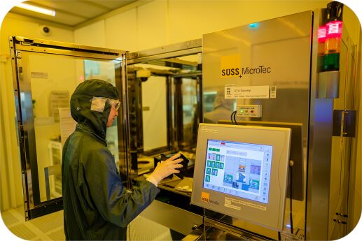
For our example process we will use a standard 4” silicon wafer and coat it with 180 nm CSAR on the fully automatic Gamma E-beam & UV coater using recipe 4318. A video demonstrating usage of our Gamma coaters can be found here. Bear in mind the video shows the UV resist coater and not the E-beam resist coater but they are identical in operation.
|
|
2", 4" and 6" substrates can be coated with AR-P6200.09 (CSAR) on Spin Coater: Gamma E-beam & UV. |
Pattern preparation
In order to expose a pattern it must be converted to V30 format (JEOL52 V3.0) using Beamer. Beamer can read several different file formants, we recommend using GDS as your input format. Beamer can do a lot of different operations on a pattern to better optimise it for writing. In this guide we will skip all of these operations and simply export the GDS pattern to a V30 file. For more advanced functionality and pattern preparation please refer to our Beamer pattern preparation guide.
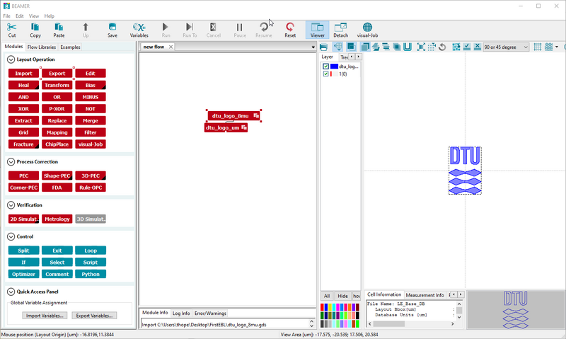
Beamer uses a node based system where each node performs an action on the pattern. In this simple example we will just have an import node to import our GDS file and connect it to an export node to output it as V30. The setup is thus as simple as can be and will look like below, the left hand side shows the simple node setup while the right side shows the pattern which in this case is a DTU logo.
|
|
Beamer uses a node based system where nodes are applied in sequence. In this example there is only an import and an export node. |
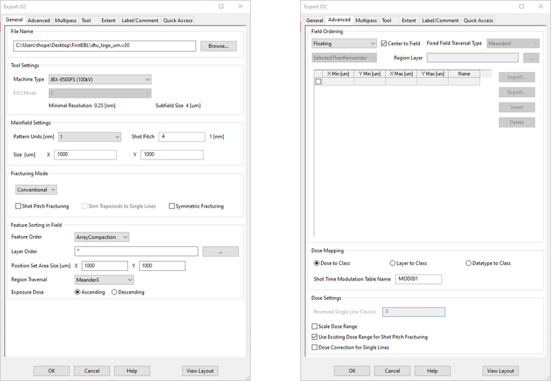
Each node has several options and these can be changed by double clicking the node. For the export node we will need to choose the correct machine in "Machine Type", the DTU Nanolab system is "JBX-9500FS (100kV)". On the advanced tab we will choose "Floating" field ordering and "Center to Field". This will ensure that our features/pattern will be written in the center of the writing field. The setup will look like the parameters below.
|
|
Beamer uses a node based system where nodes are applied in sequence. In this example there is only an import and an export node. |
Beamer is available on the preparation PC in the cleanroom and on the external Beamer PC (DTU-EM00AWQD) by Remote Desktop. Please book the External Beamer PC in Labmanager in order to use it.
SDF and JDF file preparation
In order to execute the pattern writing a significant number of parameters must be defined for the job. These are defined in two text files; the Schedule File (SDF) and Jobdeck File (JDF). The system has a close to zero tolerance on syntax error from the user and thus these files should be prepared carefully, usually by using templates and correcting the parameters to suit the exposure. We encourage users to download and use SuperEdi for editing SDJ/JDF files. As the JEOL 9500 is operated from a Unix computer you must save your SDF/JDF files in Unix format, available as an option from the “Save As” menu in SuperEdi.
The SDF is the governing job descriptor. It defines which cassette to use for exposure, which slot of that cassette to expose, which beam current to expose with and the base dose of the exposure. The SDF will reference the JDF with further job information such as which pattern to write and where to write the pattern. The JDF will in turn reference a (or set of) V30 pattern files that hold the pattern(s) to write.
For our example job we will use the following SDF. The commands are briefly described, for a more in depth explanation please consult the SDF/JDF preparation guide.
MAGAZIN    'FIRSTEBL'         The magazine name is FIRSTEBL; max. 9 capital letters

#8                            Cassette from auto stocker shelf 8 is used
%4A                           4" wafer in position A is exposed
JDF     'myfirstebl',1        Layer block no. 1 of the jdf-file 'myfirstebl.jdf' is exposed
ACC 100                       Acceleration voltage of 100keV is used (can not be changed)
CALPRM '6na_ap5'              The condition file 6na_ap5 is used, i.e. exposure at 6 nA
DEFMODE 2                     Both deflectors are used (default)
RESIST 200                    A base dose of 200 µC/cm2 is used
SHOT A,16                     Shot pitch is 16 units (of 0.25 nm), i.e. 4 nm
OFFSET(0,0)                   An offset of 0 µm is applied in both X and Y

END 8                         After exposure, cassette 8 will be remain on the stage
Pattern placement is controlled with the ARRAY command in the JDF. The goal of this example exposure is to create a dose test and thus we will use the ARRAY command to create an array of the pattern (the DTU logo) and we will use the MODULAT command to modulate the dose for each instance in the array. The ARRAY command takes six parameters as ARRAY(x,nx,dx)/(y,ny,dy), where x and y defines the center of the first element, nx and ny defines element numbers and dx and dy defines the array element pitch. The array defined in the example below will create a 10 x 1 array with an x-axis pitch of 50 µm.
Each array element is assigned a dose modulation using the MODULAT command. The MODULAT command takes two parameters as MODULAT(r,v), where r is the shot rank and v is the shot time modulation in %. The shot rank is defined during export from Beamer. For a simple design as used in this example that is not proximity corrected all elements of the pattern will be in shot rank 0. If a design is proximity corrected pattern elements will be assigned to different shot ranks. The shot time modulation is a simple percentage increase to the base dose defined by the RESIST command in the SDF. The modulation table in this example will thus expose with a base dose of 200 µC/cm2 in element (1,1) and a dose of 200 µC/cm2 + 45% = 290 µC/cm2 in element (10,1). The resulting pattern and modulation is visualised below.
JOB/W    'FIRSTEBL',4                          4inch wafer


PATH   DRF5M                                   Cyclic calibration definition
  ARRAY       (50,10,50)/(50,1,0)              10-1 array around (50,50) with 50 µm pitch in x-axis
    ASSIGN P(1)->((1,1),SHOT1)                 Pattern and modulation assignment to each array element
    ASSIGN P(1)->((2,1),SHOT2)
    ASSIGN P(1)->((3,1),SHOT3)
    ASSIGN P(1)->((4,1),SHOT4)
    ASSIGN P(1)->((5,1),SHOT5)
    ASSIGN P(1)->((6,1),SHOT6)
    ASSIGN P(1)->((7,1),SHOT7)
    ASSIGN P(1)->((8,1),SHOT8)
    ASSIGN P(1)->((9,1),SHOT9)
    ASSIGN P(1)->((10,1),SHOT10)
  AEND
PEND

LAYER  1                                      Definition of pseudo layer 1

P(1)  'dtu_logo_um.v30'                      Assignment of P(1) to V30 file
SPPRM 4.0,,,,1.0,1                            Beam parameters
STDCUR  2.2 ;nA                               Beam current + 10% overhead

SHOT1: MODULAT (( 0,0))                       Dose modulation tables
SHOT2: MODULAT (( 0,5))
SHOT3: MODULAT (( 0,10))
SHOT4: MODULAT (( 0,15))
SHOT5: MODULAT (( 0,20))
SHOT6: MODULAT (( 0,25))
SHOT7: MODULAT (( 0,30))
SHOT8: MODULAT (( 0,35))
SHOT9: MODULAT (( 0,40))
SHOT10: MODULAT (( 0,45))

END

Much more information on various commands in SDF/JDF files are available in the SDF and JDF file manual. [link]
Moving job files to exposure system
At this stage we have a V30 file containing the pattern data and an SDF and JDF file describing the exposure parameters. These must be compiled into a magazine file (.mgn) which will completely define the exposure job. Magazine files are compiled directly on the control computer and hence the V30, SDF and JDF files have to be transferred to this computer using the FFFTP client available on the support PC. For first time use FFFTP has to be setup on your user account on the support PC. This is done by the following steps:
- Login to the support PC using your DTU credentials.
- Open “FFFTP”
- Click “New connection” and fill the fields as shown in the "Host Setting" window below
- Password is "Jeoleb"
- Initial Local Folder should be your own M-drive or similar
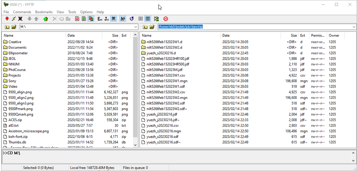
Now you can click "Connect" in FFFTP and it opens with your drive on the left side and the JEOL9500 PC on the right hand side. You can now drag and drop files between the two folders. The SDF and JDF files go in the same folder, the pattern data however goes into a separate folder. The correct folders are:
- SDF/JDF: /home/eb0/jeoleb/job/danchip
- V30: /home/eb0/jeoleb/pattern/danchipv30
Job file compilation
Once the files are transferred to the EBL control computer they can be compiled into a magazine file. The Unix interface has several desktops. Desktop one is used for EBL control and desktop two is used for file compilation. In a terminal window on desktop two the SDF, JDF and V30 files can be compiled into a MGN file with SCHD command by writing “schd -exptime sdffilename”, where the last part is the name of the actual SDF to compile.
If compilation is successful the terminal will provide a table of exposure sequences and their corresponding exposure times. Also, a .MGN file will be generated in the same folder as the SDF file. This file holds all relevant exposure information and it is this file one will load to the Expose module to initiate exposure.
If compilation does not succeed the terminal will respond with a number of errors indicating which line(s) of the SDF or JDF file is causing the error. The system is extremely sensitive to syntax error and all users will experience compilation errors. The errors can be difficult to decipher, please refer to the Compilation Error Guide. UPDATE
Job file verification
To ensure that the pattern and exposure parameters are correct the MGN file should always be verified to some extent. This can be done using the Array Check Program (ACHK) program found on the Analysis pane. The Analysis pane is usually open on the right hand side of the second desktop, if not, it can be opened from the EBX Menu. Open ACHK from the Analysis pane and click “File” -> “Open” and open your magazine file.
Sample mounting
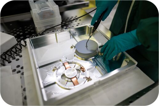
The JEOL 9500 system uses a proprietary sample cassette format and thus each sample must be mounted in an appropriate cassette. Cassettes are available for wafer sizes from 2” to 8”. Smaller chips must be mounted in dedicated chip cassettes with slots of four different sizes available. Slots are all 50 mm in width, the heights are 20, 12, 8 or 4 mm. A chip must have one side length at least 1 mm larger than the height such that it can safely be clamped in the slot. Thus the smallest possible chip to expose must have one side length of at least 5 mm.
The system is fitted with an auto stocker system that can store 10 cassettes. It is thus possible to prepare multiple substrates and define an automated job to execute exposure of several substrates across several cassettes.
Examples of cassettes are seen below. [Insert images]
For our exposure we will use a 4” cassette. The procedure is best illustrated with a video [link].
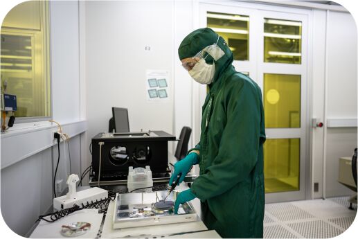
Users are allowed to unload a cassette from the auto stocker system and mount their sample(s). Users are however not allowed to put cassettes back into the auto stocker system and thus users must always contact the Nanolab E-beam loading team prior to exposure to have their cassette loaded into the auto loading system. The E-beam loading team can be contacted at [email]. Upon loading a cassette Nanolab staff will visually verify the sample has been inserted and secured correctly. Incorrect sample mounting can lead to severe damage to the internal parts of the JEOL 9500 exposure system.
Any user found to violate this rule will be permanently excluded from using the JEOL 9500 system.
 |
|
|
Samples can be loaded into appropriate cassettes on the cassette preparation table. | |
Cassette transfer
Prior to exposure the chosen cassette has to be transferred from the auto stocker system and to the main chamber. This is done from the “Loader” module on the control computer
System calibration
After cassette transfer the system has to be calibrated with the chosen beam current profile. This is done in a mostly automated sequence with only minute input from the user.
Development
Development of EBL resist can be done in two ways, either in beakers or on the automatic E-beam developer tool. The latter is equipped with ZED N50 for development of ZEP resist and AR 600-546 for development of CSAR. The system can handle chips or wafers up to 6”. It has predefined develop cycle times of 15, 30, 60 and 120 seconds.
For other developers users have to use the EBL development fumehood in E4 and manually develop their substrates in beakers of appropriate size. Please observe there are beakers dedicated solvent developers such as isopropanol and other beakers dedicated alkaline developers such as ??.
Please refer to our suggested development parameters in the table below. [table of development]
