Specific Process Knowledge/Lithography/Development/DUV developer: Difference between revisions
| Line 1: | Line 1: | ||
=Developer: TMAH Stepper = | ==Developer: TMAH Stepper== | ||
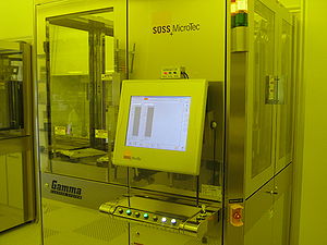
[[Image:SUSS_DEV.JPG|300x300px|right|thumb|The Developer-TMAH-Stepper is placed in F-3]] | [[Image:SUSS_DEV.JPG|300x300px|right|thumb|The Developer-TMAH-Stepper is placed in F-3]] | ||
This developer is dedicated for development of DUV resists. The developer is fully automatic and can run up to 25 substrates in a batch 4", 6", and 8" size (8" requires tool change). The machine is equipped with 1 developer line, in our case 2,38% TMAH in water (AZ 726 MIF), 1 topside rinse line with water, 1 backside rinse line with water and 1 N2 line for drying. | This developer is dedicated for development of DUV resists. The developer is fully automatic and can run up to 25 substrates in a batch 4", 6", and 8" size (8" requires tool change). The machine is equipped with 1 developer line, in our case 2,38% TMAH in water (AZ 726 MIF), 1 topside rinse line with water, 1 backside rinse line with water and 1 N2 line for drying. | ||
The user manual and contact information can be found in [http://labmanager.dtu.dk/function.php?module=Machine&view=view&mach=328 LabManager] - '''requires login''' | |||
<br clear="all" /> | <br clear="all" /> | ||
==Process information== | ===Process information=== | ||
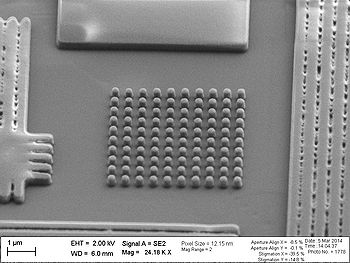
[[Image:140 250 nm tilt22 (1).jpg|350x350px|right|thumb|The SEM picture of 250 nm pillars and lines. Exposure dose is 140 J/m2.]] | [[Image:140 250 nm tilt22 (1).jpg|350x350px|right|thumb|The SEM picture of 250 nm pillars and lines. Exposure dose is 140 J/m2.]] | ||
The development process will be performed by the customer together with the Photolith group of DTU Nanolab. In case you would like to do DUV lithography please contact Lithography team, who will consult you and run your wafers together with you. | The development process will be performed by the customer together with the Photolith group of DTU Nanolab. In case you would like to do DUV lithography please contact Lithography team, who will consult you and run your wafers together with you. | ||
| Line 14: | Line 14: | ||
Here you can find a [[media:250nm_ines_and_pillars_after_developing_i_60sec.pdf| chart]] demonstrating a dependence between 250 nm line width/pillars diameter and exposure dose. | Here you can find a [[media:250nm_ines_and_pillars_after_developing_i_60sec.pdf| chart]] demonstrating a dependence between 250 nm line width/pillars diameter and exposure dose. | ||
==Standard processes== | ===Standard processes=== | ||
Post-exposure bake sequences: | Post-exposure bake sequences: | ||
| Line 37: | Line 37: | ||
<br clear="all" /> | <br clear="all" /> | ||
== Equipment performance and process related parameters == | ===Equipment performance and process related parameters=== | ||
{| border="2" cellspacing="0" cellpadding="2" | {| border="2" cellspacing="0" cellpadding="2" | ||
Revision as of 09:46, 3 February 2023
Developer: TMAH Stepper

This developer is dedicated for development of DUV resists. The developer is fully automatic and can run up to 25 substrates in a batch 4", 6", and 8" size (8" requires tool change). The machine is equipped with 1 developer line, in our case 2,38% TMAH in water (AZ 726 MIF), 1 topside rinse line with water, 1 backside rinse line with water and 1 N2 line for drying.
The user manual and contact information can be found in LabManager - requires login
Process information

The development process will be performed by the customer together with the Photolith group of DTU Nanolab. In case you would like to do DUV lithography please contact Lithography team, who will consult you and run your wafers together with you.
Here you can find a chart demonstrating a dependence between 250 nm line width/pillars diameter and exposure dose.
Standard processes
Post-exposure bake sequences:
- (1000) DCH PEB 130C 60s 60s baking at 130°C; 20s cooling
- (1001) DCH PEB 130C 90s 90s baking at 130°C; 20s cooling
Development sequences:
- (1004) DCH DEV 60s 60s single puddle development
Combined PEB and development sequences:
- (1002) DCH PEB_60s and DEV_60s 60s baking at 130°C followed by 60s single puddle development
- (1003) DCH PEB_90s and DEV_60s 90s baking at 130°C followed by 60s single puddle development
The standard developer process consists of:
- pre-wetting with water (2.5s @ 1000rpm)
- developer dispense (2.5s @ 40rpm, corresponding to ~9ml)
- development (60s @ 0rpm)
- water rinse with BSR (5s @ 3000rpm)
- nitrogen drying (7s @ 4000rpm)
and has a cycle time of ~2 minutes
| Purpose |
Development of DUV resist: KRF M230Y and KRF M35G | ||
|---|---|---|---|
| Developer |
2,38% water based TMAH | ||
| Process parameters | Spin speed |
10 - 5000 rpm | |
| Spin acceleration |
100 - 10000 rpm/s | ||
| Hotplate temperature |
130°C for post exposure baking | ||
| Substrates | Substrate size |
| |
| Allowed materials |
| ||
| Batch |
1 - 25 | ||
