Specific Process Knowledge/Thin film deposition/thermalevaporator: Difference between revisions
Created page with "=<span style="background:#FF2800">THIS PAGE IS UNDER CONSTRUCTION</span>200px= '''Feedback to this page''': '''[mailto:pvd@danchip.dtu.dk?Sub..." |
No edit summary |
||
| Line 1: | Line 1: | ||
=<span style="background:#FF2800">THIS PAGE IS UNDER CONSTRUCTION</span>[[image:Under_construction.png|200px]]= | =<span style="background:#FF2800">THIS PAGE IS UNDER CONSTRUCTION</span>[[image:Under_construction.png|200px]]= | ||
'''Feedback to this page''': '''[mailto: | '''Feedback to this page''': '''[mailto:thinfilm@danchip.dtu.dk?Subject=Feed%20back%20from%20page%20http://labadviser.danchip.dtu.dk/index.php?title=Specific_Process_Knowledge/Thin_film_deposition/thermalevaporator click here]''' | ||
[[Category: Equipment|Thin film]] | [[Category: Equipment|Thin film]] | ||
| Line 13: | Line 13: | ||
'''The user manual, | '''The user manual, APV, technical information and contact information can be found in LabManager:''' | ||
<!-- remember to remove the type of documents that are not present --> | <!-- remember to remove the type of documents that are not present --> | ||
<!-- give the link to the equipment info page in LabManager: --> | <!-- give the link to the equipment info page in LabManager: --> | ||
[http://labmanager | [http://labmanager.dtu.dk/function.php?module=Machine&view=view&mach=404 Thermal Evaporator in LabManager] | ||
<br clear="all" /> | <br clear="all" /> | ||
==Process information== | ==Process information== | ||
====Materials for | ====Materials for thermal evaporator evaporation==== | ||
*[[Specific Process Knowledge/Thin film deposition/Deposition of Aluminium|Aluminium | *[[Specific Process Knowledge/Thin film deposition/Deposition of Aluminium|Aluminium]] | ||
*[[Specific Process Knowledge/Thin film deposition/Deposition of Silver|Silver]] | |||
*[[Specific Process Knowledge/Thin film deposition/Deposition of Germanium|Germanium]] | |||
*[[Specific Process Knowledge/Thin film deposition/Deposition of Silver|Silver | |||
*[[Specific Process Knowledge/Thin film deposition/Deposition of | |||
| Line 45: | Line 35: | ||
!style="background:silver; color:black;" align="left"|Purpose | !style="background:silver; color:black;" align="left"|Purpose | ||
|style="background:LightGrey; color:black"|Deposition of metals and silicon ||style="background:WhiteSmoke; color:black"| | |style="background:LightGrey; color:black"|Deposition of metals and silicon ||style="background:WhiteSmoke; color:black"| | ||
* | *Thermal evaporation of metals | ||
|- | |- | ||
!style="background:silver; color:black" align="left" valign="top" rowspan="2"|Performance | !style="background:silver; color:black" align="left" valign="top" rowspan="2"|Performance | ||
| Line 54: | Line 43: | ||
|style="background:LightGrey; color:black"|Deposition rate | |style="background:LightGrey; color:black"|Deposition rate | ||
|style="background:WhiteSmoke; color:black"| | |style="background:WhiteSmoke; color:black"| | ||
* | *0.5 Å/s - 5 Å/s (material dependens) | ||
|- | |- | ||
!style="background:silver; color:black" align="left" valign="top" rowspan="2"|Process parameter range | !style="background:silver; color:black" align="left" valign="top" rowspan="2"|Process parameter range | ||
| Line 68: | Line 57: | ||
|style="background:LightGrey; color:black"|Batch size | |style="background:LightGrey; color:black"|Batch size | ||
|style="background:WhiteSmoke; color:black"| | |style="background:WhiteSmoke; color:black"| | ||
* | *Up to 8" wafer | ||
*Or several smaller pieces | *Or several smaller pieces | ||
*Deposition on one side of the substrate | *Deposition on one side of the substrate | ||
Revision as of 15:17, 12 October 2017
THIS PAGE IS UNDER CONSTRUCTION
Feedback to this page: click here
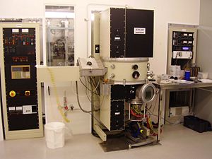
Alcatel - A system for deposition of metals

The user manual, APV, technical information and contact information can be found in LabManager:
Thermal Evaporator in LabManager
Process information
Materials for thermal evaporator evaporation
| Purpose | Deposition of metals and silicon |
|
|---|---|---|
| Performance | Film thickness |
|
| Deposition rate |
| |
| Process parameter range | Process Temperature |
|
| Process pressure |
| |
| Substrates | Batch size |
|
| Substrate material allowed |
| |
| Material allowed on the substrate |
|
* For thicknesses above 200 nm permission is requested.
