LabAdviser/314/Microscopy 314-307/SEM/Nova/Micro 4-point probe: Difference between revisions
mNo edit summary |
|
(No difference)
| |
Revision as of 08:55, 28 May 2020
4-point probe theory
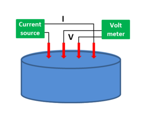
The electrical resistivity of metallic bulk and thin-film samples is usually measured by the 4-point probe technique. The classic arrangement, visible in Fig. 1, consists of four needle-like electrodes in a linear arrangement, with a current injected into the material via the outer two electrodes, while the resulting difference in electric potential is measured via the two inner electrodes.

By using separate electrodes for the current injection and for the determination of the electric potential, the contact resistance between the metal electrodes and the material does not show up in the measured results. Since the contact resistance can be large and can strongly depend on the condition and materials of the electrodes, it is easier to interpret the data measured by the 4-point probe technique than from a 2-point probe system. If the sample has a finite size and if the spacing between the probes is s1= s2 = s3 = s, the resistivity is given by:
ρ = 2aπsV/I (1)
where a is the thickness correction factor for thicknesses t equal to or less than half the probe spacing (t/s < 0.5):
a = 0.72t/s (2)
Substituting Eq. 2 in Eq. 1 we get:
ρ = 2aπsV/I = 4.53V/I (3)
If both sides of Eq. 3 are divided by t we get:
Rs = ρ/t = 4.53V/I (4)
which we refer to as sheet resistance. When the thickness t is very small respect to the spacing s, Rs is the preferred measurement quantity, being independent of any geometrical dimension and therefore a function of the material alone.
Micro 4-point probe
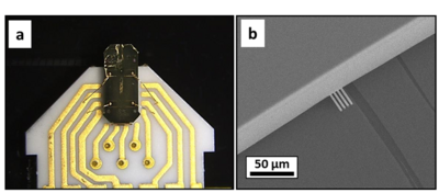
In this thesis, a variation of the classic 4-point probe method was used, called micro 4-point probe (μ4PP). This because the electrodes of the 4-point probe can easily scratch a metallic film with thickness in the nm range, thus reaching the substrate and giving inaccurate electrical measurements as result. Fig. 2a shows a μ4PP probe chip. Visible are the ceramic substrate, the Ag/Pd connector strips and the Si base from which the four cantilevers extend. For the movements, the probe chip is connected to a micromanipulator inside a SEM. Aided by SEM imaging, the probe gently touches the thin-film surface in 2-point probe mode without scratching it, followed by the collection of the data in 4-point probe mode (Fig. 2b).

Kleindiek micromanipulator
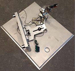
The Kleindiek Nanotechnik MM3A-EM is a plug and play micromanipulator for SEM/FIB applications, with a versatile range of modular plug-ins. The MM3A-EM can be used in most SEM/FIB instruments and offers fast setup and removal. The system consists of a base over which the micromanipulator arm is mounted (Fig. 3). The base can be attached to the SEM front door by two exagonal head screws (Fig. 4).The arm is connected to the external power supply through two plug-ins on a PCB board mounted on the SEM door.
-
Fig. 3: the base with the micromanipulator mounted on it.
-
Fig. 4: the micromanipulator mounted on the Nova NanoSEM door.
Controlling the MM3A
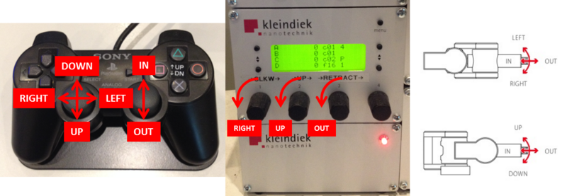
The MM3A can be controlled in two ways: using the Joypad or the Nanocontroller. The possible micromanipulator movements are shown in Fig. 5. The two controllers can control in either fine or coarse mode depending on the speed selection. There are six speeds available, three in coarse mode and three in fine mode.

Capres M4PP SEM Module
The Capres M4PP SEM Module expands the capabilities of standard Scanning Electron Microscopes (SEM) with in-situ Microscopic Four Point Probing (M4PP). The M4PP SEM Module consists of a probe holder that attaches to a micro manipulator inside the SEM chamber, a stand-alone instrumentation unit, and software for control and data acquisition.
The range of applications can vary from surface layer transport measurement to interconnect probing, to sheet resistance characterization, to characterization of inhomogeneous or microstructured advanced materials e.g. ultra-thin films and nanowires.
Module schematic


