Specific Process Knowledge/Thin film deposition/Furnace LPCVD TEOS: Difference between revisions
Appearance
No edit summary |
No edit summary |
||
| Line 1: | Line 1: | ||
Ikke skevet! | |||
==LPCVD (Low Pressure Chemical Vapor Deposition) TEOS== | ==LPCVD (Low Pressure Chemical Vapor Deposition) TEOS== | ||
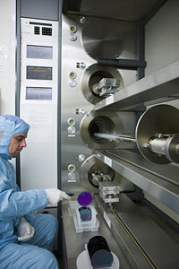
[[Image:160904_danchip_4538.jpg|300x300px|thumb|B3 Furnace LPCVD TEOS: positioned in cleanroom 2]] | [[Image:160904_danchip_4538.jpg|300x300px|thumb|B3 Furnace LPCVD TEOS: positioned in cleanroom 2]] | ||
Revision as of 14:23, 28 January 2008
Ikke skevet!
LPCVD (Low Pressure Chemical Vapor Deposition) TEOS

At the moment there is one furnace for TEOS oxide depositions at Danchip. The furnace is a Tempress horizontal furnace. The process is a batch process meaning you can run a batch of 25 wafers at a time. The deposition takes place at temperatures of 800-835 degrees Celsius. The reactive gases are dinitrogenoxide and silane. The LPCVD TEOS has a good step coverage and the film thickness is very uniform over the wafer. We have two standard LPCVD TEOS processes: One for depositing ? and one for deposition of ?. To get information on how to operate the furnace please read the manual which is uploaded to LabManager.
Process Knowledge
Please take a look at the process side for deposition of ?:
Deposition of Silicon Nitride using LPCVD
| Purpose | Deposition of TEOS silicon oxide | . |
|---|---|---|
| Performance | Film thickness |
|
| . | Step coverage |
|
| . | Film quality |
|
| Process parameter range | Process Temperature |
|
| . | Process pressure |
|
| . | Gas flows |
|
| Substrates | Batch size |
|
| . | Substrate material allowed |
|
