Specific Process Knowledge/Thin film deposition/Deposition of Zinc: Difference between revisions
| (16 intermediate revisions by 3 users not shown) | |||
| Line 1: | Line 1: | ||
'''Feedback to this page''': '''[mailto:labadviser@ | '''Feedback to this page''': '''[mailto:labadviser@nanolab.dtu.dk?Subject=Feed%20back%20from%20page%20http://labadviser.nanolab.dtu.dk/index.php?title=Specific_Process_Knowledge/Thin_film_deposition/Deposition_of_Zinc click here]''' | ||
<i> Except where otherwise stated, this page is written by <b>DTU Nanolab staff</b></i> | |||
[[Category: Equipment|Thin film]] | [[Category: Equipment|Thin film]] | ||
| Line 6: | Line 8: | ||
==Zinc deposition== | ==Zinc deposition== | ||
Zinc is tricky to deposit in a multiuser vacuum system because it has a relatively high vapor pressure at low temperatures, which means that once Zn is inside it easily re-evaporates and contaminates films of other materials. Additionally, Zn | Zinc is tricky to deposit in a multiuser vacuum system because it has a relatively high vapor pressure at low temperatures, which means that once Zn is inside it easily re-evaporates and contaminates films of other materials. Additionally, we are not keen to deposit Zn in systems with cryo pumps, as it may clog the pumping system. A final consideration is that ZnO forms on the surface of Zn and needs a higher temperature to evaporate than the Zn itself, so once the ZnO is gone, the Zn within may evaporate rapidly, making it hard to control the deposition rate. For this reason it is better to use sputtering than evaporation to deposit Zn. | ||
'''The best solution is therefore a sputter system that is pumped by a turbo pump in a chamber where Zn contamination is not a problem for other users.''' | '''The best solution is therefore a sputter system that is pumped by a turbo pump in a chamber where Zn contamination is not a problem for other users.''' | ||
Unfortunately, | Unfortunately, at Nanolab the only physical vapor deposition system with no cryo pump is the Lesker Thermal Evaporator, so this is the only system we have considered for Zn evaporation. We tested it and found that Zn coats every surface in the chamber and re-evaporates during subsequent evaporation of other materials, contaminating the growing film. After a thorough chamber cleaning, we no longer detect Zn by XPS in Al or Ag films made in the evaporator. However, this kind of cleaning takes a full working day and while the chamber is used for Zn no other materials can be deposited without contamination. '''We are therefore hesitant to use the evaporator for Zn again. If you wish to deposit Zn, please first explore other options.''' | ||
Note that Zn will not adhere to | Note that Zn will not adhere to a Si wafer (probably due to SiO2 on the surface). The same is true for a Ti-coated wafer. We were able to deposit Zn on a Ti/Au coated dummy wafer. A user was able to deposit on InGaP and InP. | ||
===XPS of Al films to detect Zn=== | ===XPS of Al films to detect Zn=== | ||
XPS was done at | ''Measurements made by Rebecca Ettlinger in June/July 2018.'' | ||
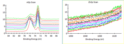
XPS was done at Nanolab with the XPS K-alpha using 50 eV and 50 ms dwell per scan. The number of scans per element varied as shown below in the figure captions. We can clearly see that the Zn amount in the Al film decreased and became indetectable after cleaning the chamber. Of course we cannot guarantee that there is no Zn contamination at all, since there is a detection limit for the XPS even with many scans per level. | |||
[[File:Al w Zn from 20-06-2018.png|400px|left|thumb|XPS of Al film made before chamber was cleaned after Zn deposition. 10 scans per level. Zn peaks are obvious. The Zn content was up to 10 % in some layers.]] | [[File:Al w Zn from 20-06-2018.png|400px|left|thumb|XPS of Al film made before chamber was cleaned after Zn deposition. 10 scans per level. Zn peaks are obvious. The Zn content was up to 10 % in some layers.]] | ||
[[File:Al wo Zn from 09-07-2018.png|400px| | [[File:Al wo Zn from 09-07-2018.png|400px|left|thumb|XPS of Al film made after chamber was cleaned after Zn deposition and a new crucible was used for Al. 10 scans per level for Al, 30 scans per level for Zn. No Zn peaks are visible.]] | ||
<br clear="all" /> | <br clear="all" /> | ||
===Lessons for future thermal deposition of Zn=== | ===Lessons for future thermal deposition of Zn (by Rebecca Ettlinger) === | ||
*It is better to use a crucible rather than a W boat to heat small Zn pellets, as the pellets sometimes jumped out of the boat when they got hot. | *It is better to use a crucible rather than a W boat to heat small Zn pellets, as the pellets sometimes jumped out of the boat when they got hot. | ||
* | *Consider using manual mode as the power level for evaporation was not always consistent and the rate was not constant even at a constant power level. See further below, however. | ||
*We needed about 12-13 % power on the Lesker Thermal evaporator to get Zn evaporation. It is best to soak for a long time(e.g., ramping and soaking for more than 5-8 minutes). | *We needed about 12-13 % power on the Lesker Nano36 Thermal evaporator to get Zn evaporation. It is best to soak for a long time(e.g., ramping and soaking for more than 5-8 minutes). | ||
*The thickness /rate measurement may not have been accurate as the crystal monitor looked irregularly coated after the deposition. | *The thickness /rate measurement may not have been accurate as the crystal monitor looked irregularly coated after the deposition. | ||
| Line 31: | Line 35: | ||
When we asked other labs about Zn evaporation, they mostly said to try to avoid it and perhaps to try to cool the substrate. An employee at the UCSB Nanofabrication Facility had tried thermal evaporation of Zn and says that their chamber now has status as Zn contaminated, but they have had no user complaints and it is now a long time since they did the deposition. Their chamber is mostly used for III-V materials. They used wires of Zn rather than pellets. | When we asked other labs about Zn evaporation, they mostly said to try to avoid it and perhaps to try to cool the substrate. An employee at the UCSB Nanofabrication Facility had tried thermal evaporation of Zn and says that their chamber now has status as Zn contaminated, but they have had no user complaints and it is now a long time since they did the deposition. Their chamber is mostly used for III-V materials. They used wires of Zn rather than pellets. | ||
More information can be found on the O-drive of the Thin film group under PVD/Thermal evaporator (for | More information can be found on the O-drive of the Thin film group under PVD/Thermal evaporator (for Nanolab staff only). | ||
===Further lessons | ===Further lessons by Chanju Kim=== | ||
''Depositions carried out in October 2018.'' | ''Depositions carried out in October 2018.'' | ||
Small Zn pellets (Lesker) were evaporated from an alumina crucible in Source 1 of the Lesker Thermal evaporator onto InP dummy substrates and InGaP substrates. | Small Zn pellets (Lesker) were evaporated from an alumina crucible in Source 1 of the Lesker Thermal evaporator onto InP dummy substrates and InGaP substrates. | ||
It was possible to use an automatic program after some adjustments. A stable deposition rate of 0.5 Å/s was obtained with a max. power of 14.5 % after approx. 15 min of ramping and soaking. The final PID parameters were P 15, I 2 and D 1. | It was possible to use an automatic program after some adjustments. A stable deposition rate of 0.5 Å/s was obtained with a max. power of 14.5 % after approx. 15 min of ramping and soaking. Depositions at 0.3 Å/s and 1 Å/s were not stable. The final PID parameters were P 15, I 2 and D 1. | ||
[[File:Zn dep rates.png|400px|left|thumb|Deposition rate versus power for four different trials with Zn deposition. Work and graph by Chanju Kim.]] | |||
It is important not to use too high power as this will give a very fast increase in the deposition rate once the evaporation is started. For new Zn pellets, an oxide removal run is recommended before the actual deposition. The max power needs to be slightly adjusted for this run (slightly higher than for already-melted pellets). | |||
Frequently exchange the QCM crystal (quartz crystal monitor) which is used to measure the thickness of the deposited film. After about 1 micron accumulated deposition, the crystal severely underestimated the thickness, whereas a fresh sensor measured accurately. The film thickness was verified with Dektak profilometry. Read more about quartz crystal monitors [[Specific_Process_Knowledge/Thin_film_deposition/Temescal#Deposition_rate_and_thickness_measurement_accuracy|here]]. | |||
[[File:QCM.png|400px|right|thumb|The quartz crystal monitor at the back of the machine, which should be exchanged frequently.]] | |||
Latest revision as of 14:40, 5 August 2025
Feedback to this page: click here
Except where otherwise stated, this page is written by DTU Nanolab staff
Zinc deposition
Zinc is tricky to deposit in a multiuser vacuum system because it has a relatively high vapor pressure at low temperatures, which means that once Zn is inside it easily re-evaporates and contaminates films of other materials. Additionally, we are not keen to deposit Zn in systems with cryo pumps, as it may clog the pumping system. A final consideration is that ZnO forms on the surface of Zn and needs a higher temperature to evaporate than the Zn itself, so once the ZnO is gone, the Zn within may evaporate rapidly, making it hard to control the deposition rate. For this reason it is better to use sputtering than evaporation to deposit Zn. The best solution is therefore a sputter system that is pumped by a turbo pump in a chamber where Zn contamination is not a problem for other users.
Unfortunately, at Nanolab the only physical vapor deposition system with no cryo pump is the Lesker Thermal Evaporator, so this is the only system we have considered for Zn evaporation. We tested it and found that Zn coats every surface in the chamber and re-evaporates during subsequent evaporation of other materials, contaminating the growing film. After a thorough chamber cleaning, we no longer detect Zn by XPS in Al or Ag films made in the evaporator. However, this kind of cleaning takes a full working day and while the chamber is used for Zn no other materials can be deposited without contamination. We are therefore hesitant to use the evaporator for Zn again. If you wish to deposit Zn, please first explore other options.
Note that Zn will not adhere to a Si wafer (probably due to SiO2 on the surface). The same is true for a Ti-coated wafer. We were able to deposit Zn on a Ti/Au coated dummy wafer. A user was able to deposit on InGaP and InP.
XPS of Al films to detect Zn
Measurements made by Rebecca Ettlinger in June/July 2018.
XPS was done at Nanolab with the XPS K-alpha using 50 eV and 50 ms dwell per scan. The number of scans per element varied as shown below in the figure captions. We can clearly see that the Zn amount in the Al film decreased and became indetectable after cleaning the chamber. Of course we cannot guarantee that there is no Zn contamination at all, since there is a detection limit for the XPS even with many scans per level.


Lessons for future thermal deposition of Zn (by Rebecca Ettlinger)
- It is better to use a crucible rather than a W boat to heat small Zn pellets, as the pellets sometimes jumped out of the boat when they got hot.
- Consider using manual mode as the power level for evaporation was not always consistent and the rate was not constant even at a constant power level. See further below, however.
- We needed about 12-13 % power on the Lesker Nano36 Thermal evaporator to get Zn evaporation. It is best to soak for a long time(e.g., ramping and soaking for more than 5-8 minutes).
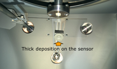
- The thickness /rate measurement may not have been accurate as the crystal monitor looked irregularly coated after the deposition.
Note that Zn sublimes.
When we asked other labs about Zn evaporation, they mostly said to try to avoid it and perhaps to try to cool the substrate. An employee at the UCSB Nanofabrication Facility had tried thermal evaporation of Zn and says that their chamber now has status as Zn contaminated, but they have had no user complaints and it is now a long time since they did the deposition. Their chamber is mostly used for III-V materials. They used wires of Zn rather than pellets. More information can be found on the O-drive of the Thin film group under PVD/Thermal evaporator (for Nanolab staff only).
Further lessons by Chanju Kim
Depositions carried out in October 2018.
Small Zn pellets (Lesker) were evaporated from an alumina crucible in Source 1 of the Lesker Thermal evaporator onto InP dummy substrates and InGaP substrates.
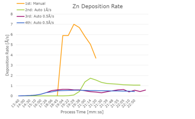
It was possible to use an automatic program after some adjustments. A stable deposition rate of 0.5 Å/s was obtained with a max. power of 14.5 % after approx. 15 min of ramping and soaking. Depositions at 0.3 Å/s and 1 Å/s were not stable. The final PID parameters were P 15, I 2 and D 1.

It is important not to use too high power as this will give a very fast increase in the deposition rate once the evaporation is started. For new Zn pellets, an oxide removal run is recommended before the actual deposition. The max power needs to be slightly adjusted for this run (slightly higher than for already-melted pellets).
Frequently exchange the QCM crystal (quartz crystal monitor) which is used to measure the thickness of the deposited film. After about 1 micron accumulated deposition, the crystal severely underestimated the thickness, whereas a fresh sensor measured accurately. The film thickness was verified with Dektak profilometry. Read more about quartz crystal monitors here.

