Specific Process Knowledge/Etch/DRIE-Pegasus/processA: Difference between revisions
| Line 188: | Line 188: | ||
<gallery caption="Optical images of the C01549 batch that is processed 20:10 mins." widths="250" heights="200" perrow="3"> | <gallery caption="Optical images of the C01549 batch that is processed 20:10 mins." widths="250" heights="200" perrow="3"> | ||
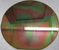
image:C01549.01-A.jpg|Wafer C01549.01: 5 % exposed area | image:C01549.01-A.jpg|Wafer C01549.01: 5 % exposed area. Some 190 nm of 600 nm oxide remains. | ||
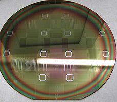
image:C01549.02-A.jpg|Wafer C01549.02: 10 % exposed area | image:C01549.02-A.jpg|Wafer C01549.02: 10 % exposed area. Some 122 nm oxide remains. | ||
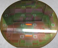
image:C01549.03.jpg|Wafer C01549.03: 20 % exposed area | image:C01549.03.jpg|Wafer C01549.03: 20 % exposed area. In the centre some 90 nm oxide remains. | ||
image:C01549.04-A.jpg|Wafer C01549.04: 35 % exposed area | image:C01549.04-A.jpg|Wafer C01549.04: 35 % exposed area. In the centre some 90 nm oxide remains. | ||
image:C01549.04-B.jpg|Wafer C01549.05: 35 % exposed area (close-up) | image:C01549.04-B.jpg|Wafer C01549.05: 35 % exposed area (close-up). The oxide has disappeared leaving the Si exposed. | ||
</gallery> | </gallery> | ||
The etching of silicon releases energy. This means that the faster the etch is, the more heat needs to be dissipated. Similarly, the larger a percentage of the wafer is etched, the more heat must be dissipated. Process A is the fastest etch and as seen above, the exposed area also plays an important role. The | |||
Revision as of 14:57, 4 February 2013
Process A
Process A is labelled Large trench (80μm wide) 150μm depth. In the acceptance test the process was run on a 150 mm SPTS wafer with 12-13 % etch load.
| Parameter | Specification | Average result |
|---|---|---|
| Etch rate (µm/min) | > 15 | 18.9 |
| Etched depth (µm) | 150 | 189.1 |
| Scallop size (nm) | < 800 | 718 |
| Profile (degs) | 91 +/- 1 | 91.1 |
| Selectivity to AZ photoresist | > 150 | 310 |
| Undercut (µm) | <1.5 | 0.84 |
| Uniformity (%) | < 3.5 | 3.0 |
| Repeatability (%) | <4 | 0.43 |
The process developed by SPTS that fulfilled these criteria had the following parameters:
| Step 1 | Step 2 | |||
|---|---|---|---|---|
| Parameter | Etch | Dep | Etch | Dep |
| Gas flow (sccm) | SF6 350 (1.5 s) 550 | C4F8 200 | SF6 350 (1.5 s) 550 | C4F8 200 |
| Cycle time (secs) | 7.0 | 4.0 | 7.0 | 4.0 |
| Pressure (mtorr) | 25 (1.5 s) 90 >> 150 | 25 | 25 (1.5 s) 150 | 25 |
| Coil power (W) | 2800 | 2000 | 2800 | 2000 |
| Platen power (W) | 120 >> 140 (1.5) 45 | 0 | 140 (1.5) 45 | 0 |
| Cycles | 11 (keep fixed) | 44 (vary this) | ||
| Common | Temperature 20 degs, HBC 10 torr, Short funnel, with baffle & 5mm spacers | |||
Process A performance
The perfomance of Process A has been investigated as a function of feature size and etch load.
Experiment
A number of wafers are patterned with the travka masks in AZ photoresist or 600 nm oxide. The wafers are then etched (batch recipe with 5 minute TDESC interstep cleans) using two different durations of process A in the DRIE-Pegasus.
|
|
Results: Optical images
- Optical images of the C01548 batch that is processed 10:05 mins.
Wafer C01548.01: 5 % exposed area
Wafer C01548.02: 10 % exposed area
Wafer C01548.03: 20 % exposed area

Wafer C01548.04: 35 % exposed area

Wafer C01548.05: 50 % exposed area
- Without pre-etch measurements of the thicknesses of the photoresist it is not possible to determine the resist etch rate. However, it looks very uniform.


- Optical images of the C01549 batch that is processed 20:10 mins.

Wafer C01549.01: 5 % exposed area. Some 190 nm of 600 nm oxide remains.

Wafer C01549.02: 10 % exposed area. Some 122 nm oxide remains.

Wafer C01549.03: 20 % exposed area. In the centre some 90 nm oxide remains.

Wafer C01549.04: 35 % exposed area. In the centre some 90 nm oxide remains.
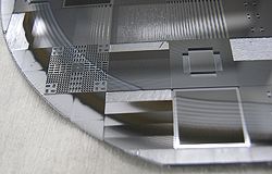
Wafer C01549.05: 35 % exposed area (close-up). The oxide has disappeared leaving the Si exposed.


The etching of silicon releases energy. This means that the faster the etch is, the more heat needs to be dissipated. Similarly, the larger a percentage of the wafer is etched, the more heat must be dissipated. Process A is the fastest etch and as seen above, the exposed area also plays an important role. The