Specific Process Knowledge/Etch/DRIE-Pegasus/processA: Difference between revisions
Jump to navigation
Jump to search
| Line 184: | Line 184: | ||
image:C01548.04-A.jpg|Wafer C01548.01: 35 % exposed area | image:C01548.04-A.jpg|Wafer C01548.01: 35 % exposed area | ||
image:C01548.05-A.jpg|Wafer C01548.01: 50 % exposed area | image:C01548.05-A.jpg|Wafer C01548.01: 50 % exposed area | ||
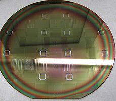
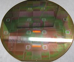
Without pre-etch measurements of the thicknesses of the photoresist it is not possible to determine the resist etch rate. However, it looks very uniform. | |||
</gallery> | </gallery> | ||
Revision as of 12:57, 4 February 2013
Process A
Process A is labelled Large trench (80μm wide) 150μm depth. In the acceptance test the process was run on a 150 mm SPTS wafer with 12-13 % etch load.
| Parameter | Specification | Average result |
|---|---|---|
| Etch rate (µm/min) | > 15 | 18.9 |
| Etched depth (µm) | 150 | 189.1 |
| Scallop size (nm) | < 800 | 718 |
| Profile (degs) | 91 +/- 1 | 91.1 |
| Selectivity to AZ photoresist | > 150 | 310 |
| Undercut (µm) | <1.5 | 0.84 |
| Uniformity (%) | < 3.5 | 3.0 |
| Repeatability (%) | <4 | 0.43 |
The process developed by SPTS that fulfilled these criteria had the following parameters:
| Step 1 | Step 2 | |||
|---|---|---|---|---|
| Parameter | Etch | Dep | Etch | Dep |
| Gas flow (sccm) | SF6 350 (1.5 s) 550 | C4F8 200 | SF6 350 (1.5 s) 550 | C4F8 200 |
| Cycle time (secs) | 7.0 | 4.0 | 7.0 | 4.0 |
| Pressure (mtorr) | 25 (1.5 s) 90 >> 150 | 25 | 25 (1.5 s) 150 | 25 |
| Coil power (W) | 2800 | 2000 | 2800 | 2000 |
| Platen power (W) | 120 >> 140 (1.5) 45 | 0 | 140 (1.5) 45 | 0 |
| Cycles | 11 (keep fixed) | 44 (vary this) | ||
| Common | Temperature 20 degs, HBC 10 torr, Short funnel, with baffle & 5mm spacers | |||
Process A performance
The perfomance of Process A has been investigated as a function of feature size and etch load.
Experiment
A number of wafers are patterned with the travka masks in AZ photoresist or 600 nm oxide. The wafers are then etched (batch recipe with 5 minute TDESC interstep cleans) using two different durations of process A in the DRIE-Pegasus.
|
|
Results
- Optical images of the C01548 batch that is processed 10:05 mins.
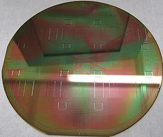
Wafer C01548.01: 5 % exposed area
Wafer C01548.02: 10 % exposed area
Wafer C01548.01: 20 % exposed area

Wafer C01548.01: 35 % exposed area

Wafer C01548.01: 50 % exposed area
- Without pre-etch measurements of the thicknesses of the photoresist it is not possible to determine the resist etch rate. However, it looks very uniform.


