Specific Process Knowledge/Characterization/XPS: Difference between revisions
| (60 intermediate revisions by 2 users not shown) | |||
| Line 1: | Line 1: | ||
'''Unless anything else is stated, everything on this page, text and pictures are made by DTU Nanolab.''' | |||
'''Feedback to this page''': '''[mailto:labadviser@ | '''All links to Kemibrug (SDS) and Labmanager Including APV and QC requires login.''' | ||
'''Feedback to this page''': '''[mailto:labadviser@nanolab.dtu.dk?Subject=Feed%20back%20from%20page%20http://labadviser.nanolab.dtu.dk/index.php?title=Specific_Process_Knowledge/Characterization/XPS click here]''' | |||
<!--Checked for updates on 14/5-2018 - ok/jmli --> | <!--Checked for updates on 14/5-2018 - ok/jmli --> | ||
{{Template:Author-jmli1}} | |||
==XPS | ==The XPS tools at DTU Nanolab== | ||
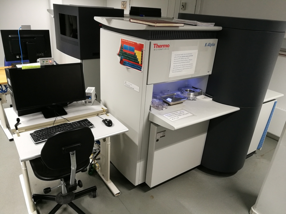
[[Image:XPS K-Alpha.jpg |frame|x300px|The K-Alpha from 2007 is one of the first instruments of this type that was produced.{{photo1}} ]] | |||
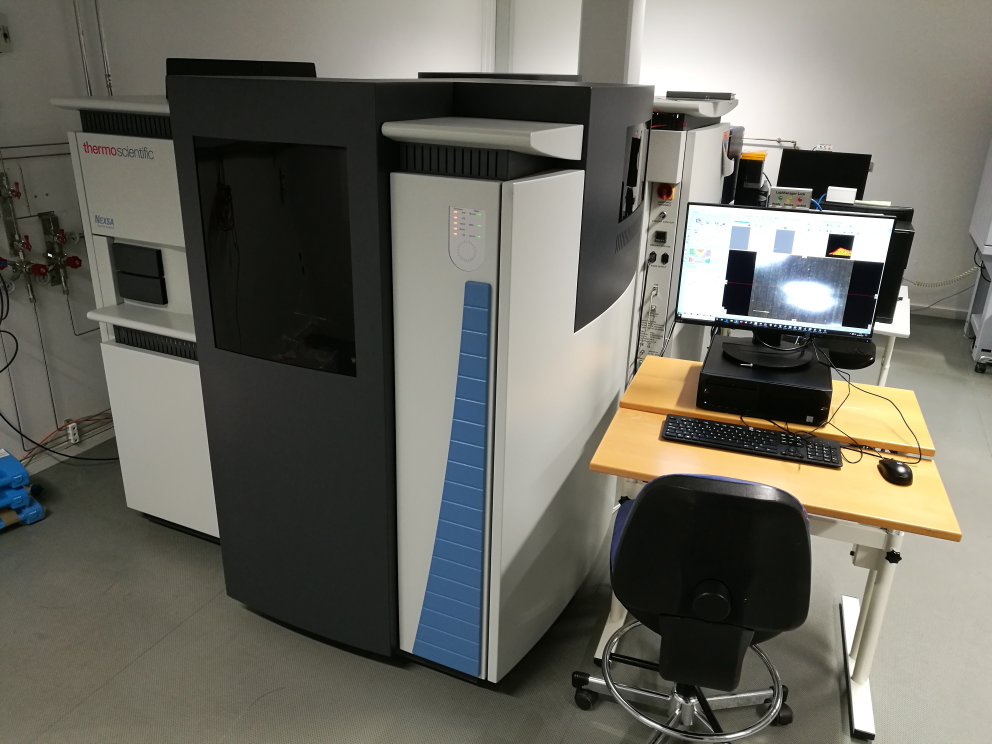
[[Image:XPS Nexsa.png |frame|x300px|The Nexsa from 2019 is on the surface very similar to the K-Alpha. Its panels, however, hide a whole range of supplementary techniques.{{photo1}} ]] | |||
In the basement under the cleanroom two X-ray Photoelectron Spectroscopy (XPS) systems are installed back-to-back in the center of room 904. They are both manufactured by Thermofisher and they enable the users to perform elemental and chemical analysis of samples. The [[Specific Process Knowledge/Characterization/XPS/K-Alpha |XPS K-Alpha]] is a base technique instrument providing XPS analysis. The [[Specific Process Knowledge/Characterization/XPS/Nexsa |XPS Nexsa]] is an upgraded version with all options. | |||
[ | * [[Specific Process Knowledge/Characterization/XPS/K-Alpha|The XPS K-Alpha page]] | ||
* [[Specific Process Knowledge/Characterization/XPS/Nexsa|The XPS Nexsa page]] | |||
==Elemental analysis== | ==Elemental analysis== | ||
The XPS instrument enables elemental analysis, chemical state analysis on the sample surface or deeper down by a depth profiling. A comparison about techniques and instruments used for elemental analysis at | The XPS instrument enables elemental analysis, chemical state analysis on the sample surface or deeper down by a depth profiling. A comparison about techniques and instruments used for elemental analysis at DTU Nanolab can be found on the page [[Specific Process Knowledge/Characterization/Element analysis|Element analysis]]. | ||
More about the different possibilities of the XPS instrument is found here: | |||
*[[Specific Process Knowledge/Characterization/XPS/XPS technique|The XPS technique]] | *[[Specific Process Knowledge/Characterization/XPS/XPS technique|The XPS technique]] | ||
*[[Specific Process Knowledge/Characterization/XPS/XPS elemental composition|Elemental analysis]] | *[[Specific Process Knowledge/Characterization/XPS/XPS elemental composition|Elemental analysis]] | ||
*[[Specific Process Knowledge/Characterization/XPS/XPS Depth profiling|Depth profiling]] | *[[Specific Process Knowledge/Characterization/XPS/XPS Depth profiling|Depth profiling]] | ||
*[[/Carbon contamination|Carbon contamination]] | *[[Specific Process Knowledge/Characterization/XPS/Carbon contamination|Carbon contamination]] | ||
*[[Specific Process Knowledge/Characterization/XPS/ExtDocs | Links to external material ]] | |||
*[[Specific Process Knowledge/Characterization/XPS/Training | Links to instruction videos ]] | |||
== Getting access to the XPS tools== | |||
Click [[Specific Process Knowledge/Characterization/XPS/Access | '''HERE''' ]] to see information on how to get access to the XPS. | |||
== Analyzing XPS spectra == | == Analyzing XPS spectra == | ||
The analysis of XPS spectra is an art in itself. | The analysis of XPS spectra is an art in itself. It can be done using various software packages available on the internet. In the links below we will focus on two such examples, Avantage and CasaXPS. | ||
*[[Specific Process Knowledge/Characterization/XPS/Processing|Processing XPS data]] | *[[Specific Process Knowledge/Characterization/XPS/SoftwareInstall|How to access XPS software: Download/install or by access to server]] | ||
*[[Specific Process Knowledge/Characterization/XPS/Processing|Processing XPS data with Avantage]] | |||
*[[Specific Process Knowledge/Characterization/XPS/Export2CasaXPS | Export Avantage data to CasaXPS]] | |||
== | ==Techniques and option on the XPS tools== | ||
{| border="2" cellspacing="0" cellpadding="1" |- | {| border="2" cellspacing="0" cellpadding="1" | ||
!style="background:silver; color:black;" align="left"|Purpose | |- | ||
|style="background:LightGrey; color:black"| | !style="background:silver; color:black;" align="left" colspan="2"|Equipment | ||
!style="background:silver; color:black;" align="left" |[[Specific Process Knowledge/Characterization/XPS/K-Alpha |XPS K-Alpha (Manufactured by Thermofisher)]] | |||
!style="background:silver; color:black;" align="left" |[[Specific Process Knowledge/Characterization/XPS/Nexsa |XPS Nexsa (Manufactured by Thermofisher)]] | |||
|- | |||
!style="background:silver; color:black;" align="left" rowspan="2"|Purpose | |||
|style="background:LightGrey; color:black"|Main | |||
|style="background:WhiteSmoke; color:black"| XPS analysis using monochromated Al-Kα radiation at 1486.6 eV | |||
|style="background:WhiteSmoke; color:black"| XPS analysis using monochromated Al-Kα radiation at 1486.6 eV | |||
|- | |||
|style="background:LightGrey; color:black"|Alternative/complementary | |||
|style="background:WhiteSmoke; color:black"| | |style="background:WhiteSmoke; color:black"| | ||
* [[Specific Process Knowledge/Characterization/XPS/ | * Work function measurements | ||
* [[Specific Process Knowledge/Characterization/XPS/ | |style="background:WhiteSmoke; color:black"| | ||
* | * Work function measurements | ||
* | * [[Specific Process Knowledge/Characterization/XPS/UPS technique| Ultraviolet Photoelectron Spectroscopy (UPS) with He I and He II UV source]] | ||
* [[Specific Process Knowledge/Characterization/XPS/ | * [[Specific Process Knowledge/Characterization/XPS/ISS|Ion Scattering Spectroscopy or ISS]] | ||
* [[Specific Process Knowledge/Characterization/XPS/REELS|Reflected Electron Energy Loss Spectroscopy or REELS]] | |||
* Angular Resolved Ultraviolet Photoelectron Spectroscopy (ARUPS) | |||
* [[Specific Process Knowledge/Characterization/XPS/Raman|Raman spectroscopy]] | |||
|- | |- | ||
!rowspan="5" style="background:silver; color:black" align="left"| Performance | !rowspan="5" style="background:silver; color:black" align="left"| Performance | ||
|style="background:LightGrey; color:black"|Spot size | |style="background:LightGrey; color:black"|Spot size | ||
|style="background:WhiteSmoke; color:black"| | |style="background:WhiteSmoke; color:black"|XPS: 30µm - 400µm | ||
|style="background:WhiteSmoke; color:black"| | |||
* XPS: 10µm - 400µm | |||
* Raman: > 15 µm | |||
|- | |- | ||
|style="background:LightGrey; color:black"| | |style="background:LightGrey; color:black"|Pass energy | ||
|style="background:WhiteSmoke; color:black"| | |style="background:WhiteSmoke; color:black"|10-400 eV | ||
|style="background:WhiteSmoke; color:black"|10-400 eV (XPS and ISS) | |||
|- | |- | ||
|style="background:LightGrey; color:black"| | |style="background:LightGrey; color:black"|Analysis modes | ||
|style="background:WhiteSmoke; color:black"| | |style="background:WhiteSmoke; color:black"|Scanned and snapshot | ||
|style="background:WhiteSmoke; color:black"|Scanned, snapshot and SnapMap | |||
|- | |- | ||
|style="background:LightGrey; color:black"|Charge compensation | |style="background:LightGrey; color:black"|Charge compensation | ||
|style="background:WhiteSmoke; color:black"| | |style="background:WhiteSmoke; color:black"| Flood gun to be used for charge compensation of non conductive samples only | ||
Flood gun | |style="background:WhiteSmoke; color:black"| Flood gun to be used for charge compensation of non conductive samples and for source of low energy electrons (REELS) | ||
|style="background:WhiteSmoke; color:black"| | |||
|- | |- | ||
|style="background:LightGrey; color:black"| | |style="background:LightGrey; color:black"|Depth profiles | ||
|style="background:WhiteSmoke; color:black"| | |style="background:WhiteSmoke; color:black"|Depth profiles with single Ar ion bombardment | ||
* Monoatomic energy range 200-3000 eV | |||
|style="background:WhiteSmoke; color:black"|Depth profiles with MonoAtomic and Gas Cluster Ion Source ([[Media:MAGCIS.pdf |MAGCIS]]) | |||
* Monoatomic energy range 200-4000 eV | |||
* Cluster mode energy range: 2-8 keV | |||
*Cluster size range: 75-2000 atoms | |||
|- | |- | ||
!rowspan="2" style="background:silver; color:black" align="left"|Substrates | !rowspan="2" style="background:silver; color:black" align="left"|Substrates / Samples | ||
|style="background:LightGrey; color:black"| | |style="background:LightGrey; color:black"|Sample holder size | ||
|style="background:WhiteSmoke; color:black"| | |style="background:WhiteSmoke; color:black"| Maximum 60x60 mm | ||
Maximum 60x60 mm | |style="background:WhiteSmoke; color:black"| Maximum 60x60 mm | ||
|- | |- | ||
| style="background:LightGrey; color:black"| | | style="background:LightGrey; color:black"|Sample height | ||
|style="background:WhiteSmoke; color:black"| | |style="background:WhiteSmoke; color:black"| Maximum 20 mm | ||
Maximum | |style="background:WhiteSmoke; color:black"| Maximum 20 mm | ||
|- | |- | ||
|} | |} | ||
Latest revision as of 15:25, 8 May 2023
Unless anything else is stated, everything on this page, text and pictures are made by DTU Nanolab.
All links to Kemibrug (SDS) and Labmanager Including APV and QC requires login.
Feedback to this page: click here
Unless otherwise stated, all content on this page was created by Jonas Michael-Lindhard, DTU Nanolab
The XPS tools at DTU Nanolab


In the basement under the cleanroom two X-ray Photoelectron Spectroscopy (XPS) systems are installed back-to-back in the center of room 904. They are both manufactured by Thermofisher and they enable the users to perform elemental and chemical analysis of samples. The XPS K-Alpha is a base technique instrument providing XPS analysis. The XPS Nexsa is an upgraded version with all options.
Elemental analysis
The XPS instrument enables elemental analysis, chemical state analysis on the sample surface or deeper down by a depth profiling. A comparison about techniques and instruments used for elemental analysis at DTU Nanolab can be found on the page Element analysis.
More about the different possibilities of the XPS instrument is found here:
Getting access to the XPS tools
Click HERE to see information on how to get access to the XPS.
Analyzing XPS spectra
The analysis of XPS spectra is an art in itself. It can be done using various software packages available on the internet. In the links below we will focus on two such examples, Avantage and CasaXPS.
- How to access XPS software: Download/install or by access to server
- Processing XPS data with Avantage
- Export Avantage data to CasaXPS
Techniques and option on the XPS tools
| Equipment | XPS K-Alpha (Manufactured by Thermofisher) | XPS Nexsa (Manufactured by Thermofisher) | |
|---|---|---|---|
| Purpose | Main | XPS analysis using monochromated Al-Kα radiation at 1486.6 eV | XPS analysis using monochromated Al-Kα radiation at 1486.6 eV |
| Alternative/complementary |
|
| |
| Performance | Spot size | XPS: 30µm - 400µm |
|
| Pass energy | 10-400 eV | 10-400 eV (XPS and ISS) | |
| Analysis modes | Scanned and snapshot | Scanned, snapshot and SnapMap | |
| Charge compensation | Flood gun to be used for charge compensation of non conductive samples only | Flood gun to be used for charge compensation of non conductive samples and for source of low energy electrons (REELS) | |
| Depth profiles | Depth profiles with single Ar ion bombardment
|
Depth profiles with MonoAtomic and Gas Cluster Ion Source (MAGCIS)
| |
| Substrates / Samples | Sample holder size | Maximum 60x60 mm | Maximum 60x60 mm |
| Sample height | Maximum 20 mm | Maximum 20 mm | |
