Specific Process Knowledge/Etch/Wet Polysilicon Etch: Difference between revisions
No edit summary |
|||
| (11 intermediate revisions by 5 users not shown) | |||
| Line 1: | Line 1: | ||
'''Feedback to this page''': '''[mailto: | '''Feedback to this page''': '''[mailto:labadviser@nanolab.dtu.dk?Subject=Feed%20back%20from%20page%20http://labadviser.nanolab.dtu.dk/index.php/Specific_Process_Knowledge/Etch/Wet_Polysilicon_Etch click here]''' | ||
'''Unless anything else is stated, everything on this page, text and pictures are made by DTU Nanolab. | |||
'''All links to Kemibrug (SDS) and Labmanager Including APV requires login.''' | |||
'''All measurements on this page has been made by Nanolab staff.''' | |||
[[Category: Equipment|Etch Wet Polysilicon]] | |||
[[Category: Etch (Wet) bath|Polysilicon]] | |||
==Wet PolySi Etch== | ==Wet PolySi Etch== | ||
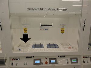
[[Image: | [[Image:polyetch1.jpg|300x300px|thumb|The 'Poly Si Etch' bath is placed inside Wet Bench 04 in cleanroom D-3]] | ||
The wet PolySi Etch is an isotropic silicon etch. This holds for both a poly-silicon thin-film as well as single-crystalline material such as a Si(100) surface. The | The wet PolySi Etch is an isotropic silicon etch. This holds for both a poly-silicon thin-film as well as single-crystalline material such as a Si(100) surface. The Poly Si Etch bath is placed inside 'Wet Bench 04: Oxide and Poly etch' cleanroom D-3. For samples that are not allowed in this bath the polysilicon etch solution can also be mixed in a plastic beaker in Fume hood 01 or 02 (Acids/bases). | ||
The PolySi Etch is typically used for opening holes in poly-silicon thin-films, using photoresist as an etch mask. Due to its isotropic nature the under-etching (etch-bias) at least amounts to the thickness of the poly-silicon layer. Another example of usage is etching of "circular-shaped" holes in silicon substrates. | The PolySi Etch is typically used for opening holes in poly-silicon thin-films, using photoresist as an etch mask or to strip Poly silicon of a wafer. Due to its isotropic nature the under-etching (etch-bias) at least amounts to the thickness of the poly-silicon layer. Another example of usage is etching of "circular-shaped" holes in silicon substrates. | ||
The PolySi Etch is based on the combined oxidation of silicon followed by | The PolySi Etch is based on the combined oxidation of silicon (by nitric acid) followed by an etch of the formed silicon oxide (by hydrofluoric acid). The etch solution consists of: | ||
HNO<sub>3</sub> : BHF : H<sub>2</sub>O - (20 : 1 : 20) | HNO<sub>3</sub> : BHF : H<sub>2</sub>O - (20 : 1 : 20) | ||
'''NB: The life time of the solution is | '''NB: The life time of the solution is a few days to 4 weeks.''' | ||
'''The user manual and contact information can be found in LabManager:''' | '''The user manual and contact information can be found in LabManager:''' | ||
<!-- remember to remove the type of documents that are not present --> | <!-- remember to remove the type of documents that are not present --> | ||
[http://labmanager.danchip.dtu.dk/function.php?module=Machine&view=view&mach= | [http://labmanager.danchip.dtu.dk/function.php?module=Machine&view=view&mach=379 Poly Si Etch info page in LabManager] | ||
===PolySi Etch data=== | ===PolySi Etch data=== | ||
| Line 56: | Line 65: | ||
!Etch rate | !Etch rate | ||
| | | | ||
*R<sub>Si</sub> ~ | *R<sub>Si</sub> ~100-200 nm/min (depending on doping level) | ||
*R<sub>SiO<sub>2</sub></sub> ~ | *R<sub>SiO<sub>2</sub></sub> ~6 nm/min | ||
*R<sub>Si<sub>3</sub>N<sub>4</sub></sub> ~0 nm/min | |||
*Photoresist (2.2 µm) withstand ~20-30 min | *Photoresist (2.2 µm) withstand ~20-30 min | ||
|- | |- | ||
| Line 70: | Line 80: | ||
!Size of substrate | !Size of substrate | ||
| | | | ||
4-6" wafers | |||
|- | |- | ||
|} | |} | ||
Latest revision as of 11:03, 7 February 2023
Feedback to this page: click here
Unless anything else is stated, everything on this page, text and pictures are made by DTU Nanolab.
All links to Kemibrug (SDS) and Labmanager Including APV requires login.
All measurements on this page has been made by Nanolab staff.
Wet PolySi Etch

The wet PolySi Etch is an isotropic silicon etch. This holds for both a poly-silicon thin-film as well as single-crystalline material such as a Si(100) surface. The Poly Si Etch bath is placed inside 'Wet Bench 04: Oxide and Poly etch' cleanroom D-3. For samples that are not allowed in this bath the polysilicon etch solution can also be mixed in a plastic beaker in Fume hood 01 or 02 (Acids/bases).
The PolySi Etch is typically used for opening holes in poly-silicon thin-films, using photoresist as an etch mask or to strip Poly silicon of a wafer. Due to its isotropic nature the under-etching (etch-bias) at least amounts to the thickness of the poly-silicon layer. Another example of usage is etching of "circular-shaped" holes in silicon substrates.
The PolySi Etch is based on the combined oxidation of silicon (by nitric acid) followed by an etch of the formed silicon oxide (by hydrofluoric acid). The etch solution consists of:
HNO3 : BHF : H2O - (20 : 1 : 20)
NB: The life time of the solution is a few days to 4 weeks.
The user manual and contact information can be found in LabManager:
Poly Si Etch info page in LabManager
PolySi Etch data
| PolySi Etch @ room temperature | |
|---|---|
| General description |
Etch of poly-si/Si(100) |
| Chemical solution | HNO3 : BHF : H2O (20 : 1 : 20) |
| Process temperature | Room temperature |
| Possible masking materials |
|
| Etch rate |
|
| Batch size |
1-25 wafers at a time |
| Size of substrate |
4-6" wafers |
