Specific Process Knowledge/Lithography/DUVStepperLithography/Optimization and Simulation: Difference between revisions
No edit summary |
No edit summary |
||
| (16 intermediate revisions by 3 users not shown) | |||
| Line 1: | Line 1: | ||
{{:Specific Process Knowledge/Lithography/authors_generic}} | |||
'''Feedback to this page''': '''[mailto:labadviser@nanolab.dtu.dk?Subject=Feed%20back%20from%20page%20http://labadviser.nanolab.dtu.dk/index.php?title=Specific_Process_Knowledge/Lithography/DUVStepperLithography/Optimization_and_Simulation click here]''' | |||
[[Category: Equipment|Lithography]] | |||
[[Category: Lithography]] | |||
__TOC__ | |||
= | == Optimization and Simulation in Deep UV lithography == | ||
In order to accomplish the best fidelity of the produced pattern on the wafer, both the characteristics of the illumination system, the exposure process and the dimensions/ shapes of the designed structures on the reticle (mask for projection lithography) must be adjusted. Different techniques can be applied to improve the resolution and the depth of focus of the illumination tool for each individual pattern. Either the mask design will be optimized with the help of optical proximity corrections (OPC) or- in a second technique -the optical illumination system will be adapted to the respective pattern. Here relevant optical parameters as the coherence of the aerial image or the numerical aperture of the projection lens can be modified, or alternatively off-axis illumination - as i.e. annular and quadrupole sources - can be used. | |||
Both, optimizing the mask design and the illumination system are useful approaches that can be exerted to achieve resist structures on the wafer with the most accurate CD control, the preferred sidewall angles, the lowest corner rounding or line end shortening. Additionally, the impact of the reaction kinetics of the resist during exposure, post exposure bake and development must be considered in order to exceed the requirements of the device to be fabricated. | |||
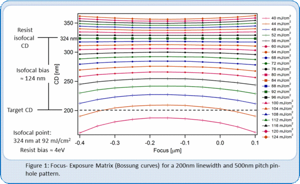
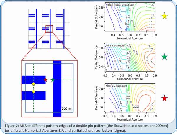
However, one of the key issues for lithographic optimization is the definition of metrics needed to classify the process quality. With the help of the Prolith™ software from KLA-Tencor the focus-exposure matrix can be used to determine a process window that leads to a maximized depth of focus for the required specification, as i.e. the desired target CD, the exposure latitude, the resist loss and/or the side-wall angles. Figure 1 shows the focus-exposure matrix of a pin-hole-array, including the relevant information obtained by a simulation, i.e. the isofocal point, the target CD, the resist bias and the isofocal bias. Secondly, with the help of the gradient-based approach, the gradients of the image that is projected and recorded into the photoresist can be used as a metric for both the achieved image and resist contrast. In Figure 2 the normalized image log-slope (NILS) is defined as the slope of the light intensity at the four different pattern edges for a double pin pattern. For each pattern edge - indicated by stars- an optimum NA or sigma value can be found leading to the larges light intensity slope at the individual edge. | |||
[[File:Focus_Exposure_Matrix.gif|600px]] [[File:NILS.gif|600px]] | |||
Latest revision as of 13:36, 3 February 2023
Specific Process Knowledge/Lithography/authors generic
Feedback to this page: click here
Optimization and Simulation in Deep UV lithography
In order to accomplish the best fidelity of the produced pattern on the wafer, both the characteristics of the illumination system, the exposure process and the dimensions/ shapes of the designed structures on the reticle (mask for projection lithography) must be adjusted. Different techniques can be applied to improve the resolution and the depth of focus of the illumination tool for each individual pattern. Either the mask design will be optimized with the help of optical proximity corrections (OPC) or- in a second technique -the optical illumination system will be adapted to the respective pattern. Here relevant optical parameters as the coherence of the aerial image or the numerical aperture of the projection lens can be modified, or alternatively off-axis illumination - as i.e. annular and quadrupole sources - can be used.
Both, optimizing the mask design and the illumination system are useful approaches that can be exerted to achieve resist structures on the wafer with the most accurate CD control, the preferred sidewall angles, the lowest corner rounding or line end shortening. Additionally, the impact of the reaction kinetics of the resist during exposure, post exposure bake and development must be considered in order to exceed the requirements of the device to be fabricated.
However, one of the key issues for lithographic optimization is the definition of metrics needed to classify the process quality. With the help of the Prolith™ software from KLA-Tencor the focus-exposure matrix can be used to determine a process window that leads to a maximized depth of focus for the required specification, as i.e. the desired target CD, the exposure latitude, the resist loss and/or the side-wall angles. Figure 1 shows the focus-exposure matrix of a pin-hole-array, including the relevant information obtained by a simulation, i.e. the isofocal point, the target CD, the resist bias and the isofocal bias. Secondly, with the help of the gradient-based approach, the gradients of the image that is projected and recorded into the photoresist can be used as a metric for both the achieved image and resist contrast. In Figure 2 the normalized image log-slope (NILS) is defined as the slope of the light intensity at the four different pattern edges for a double pin pattern. For each pattern edge - indicated by stars- an optimum NA or sigma value can be found leading to the larges light intensity slope at the individual edge.


