Specific Process Knowledge/Characterization/XPS/K-Alpha: Difference between revisions
No edit summary |
No edit summary |
||
| (6 intermediate revisions by the same user not shown) | |||
| Line 4: | Line 4: | ||
[[Category: Characterization|Chemical]] | [[Category: Characterization|Chemical]] | ||
= The XPS K-Alpha = | == The XPS K-Alpha == | ||
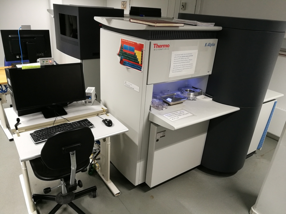
Name: XPS K-Alpha <br> | |||
Vendor: Thermofisher <br> | |||
The XPS K-Alpha allows you to analyse a broad range of samples with the XPS technique. | |||
'''The user manual(s), user APV(s), technical information and contact information are be found in LabManager:''' | '''The user manual(s), user APV(s), technical information and contact information are be found in LabManager:''' | ||
| Line 11: | Line 15: | ||
<!-- give the link to the equipment info page in LabManager: --> | <!-- give the link to the equipment info page in LabManager: --> | ||
[http://labmanager.dtu.dk/function.php?module=Machine&view=view&mach=276 XPS K-Alpha in LabManager] | [http://labmanager.dtu.dk/function.php?module=Machine&view=view&mach=276 XPS K-Alpha in LabManager] | ||
[[Image:XPS K-Alpha.jpg |frame|x300px|The K-Alpha has its back turned towards the [[Specific Process Knowledge/Characterization/XPS/Nexsa | XPS Nexsa]] in room 904 in building 346.]] | |||
==Process information== | |||
The XPS instrument enables elemental analysis, chemical state analysis on the sample surface or deeper down by a depth profiling. A comparison about techniques and instruments used for elemental analysis at DTU Nanolab can be found on the page [[Specific Process Knowledge/Characterization/Element analysis|Element analysis]]. | |||
More about the different possibilities of the XPS instrument is found here: | |||
*[[Specific Process Knowledge/Characterization/XPS/XPS technique|The XPS technique]] | |||
*[[Specific Process Knowledge/Characterization/XPS/XPS elemental composition|Elemental analysis]] | |||
*[[Specific Process Knowledge/Characterization/XPS/XPS Chemical states |Chemical sensitivity]] | |||
*[[Specific Process Knowledge/Characterization/XPS/XPS Depth profiling|Depth profiling]] | |||
*[[Specific Process Knowledge/Characterization/XPS/Carbon contamination|Carbon contamination]] | |||
*[[Specific Process Knowledge/Characterization/XPS/ExtDocs | Links to external material ]] | |||
== Getting access to the XPS == | |||
Click [[Specific Process Knowledge/Characterization/XPS/Access | '''HERE''' ]] to see information on how to get access to the XPS. | |||
== Performance of XPS K-Alpha == | |||
{| border="2" cellspacing="0" cellpadding="1" |- | |||
!style="background:silver; color:black;" align="left"|Purpose | |||
|style="background:LightGrey; color:black"|Chemical analysis | |||
|style="background:WhiteSmoke; color:black"| | |||
* [[Specific Process Knowledge/Characterization/XPS/XPS elemental composition|Probing elemental composition]] | |||
* [[Specific Process Knowledge/Characterization/XPS/XPS Chemical states |Chemical state identification]] | |||
* Non destructive technique | |||
* Surface sensitive | |||
* [[Specific Process Knowledge/Characterization/XPS/XPS Depth profiling|Depth profiling]] possible by ion beam etch of sample | |||
|- | |||
!rowspan="5" style="background:silver; color:black" align="left"| Performance | |||
|style="background:LightGrey; color:black"|Spot size | |||
|style="background:WhiteSmoke; color:black"|Can be set between 30µm - 400µm | |||
|- | |||
|style="background:LightGrey; color:black"|Probing depth | |||
|style="background:WhiteSmoke; color:black"|Depending on probed element. Max probe depth lies within 10-200 Å. | |||
|- | |||
|style="background:LightGrey; color:black"|Resolution | |||
|style="background:WhiteSmoke; color:black"|Dependent on probed elements. Concentrations down to about 0,5 atomic % can in some cases be detected. | |||
|- | |||
|style="background:LightGrey; color:black"|Charge compensation | |||
|style="background:WhiteSmoke; color:black"| | |||
Flood gun can be used for charge compensation of non conductive samples | |||
|- | |||
|style="background:LightGrey; color:black"|Finding structures | |||
|style="background:WhiteSmoke; color:black"|Choose measuring spot from camera image (magnified) | |||
|- | |||
|- | |||
|- | |||
!rowspan="2" style="background:silver; color:black" align="left"|Depth profiling | |||
|style="background:LightGrey; color:black"|Purpose | |||
|style="background:WhiteSmoke; color:black"|With ion beam etch the top layer of the material can be removed, to do a depth profiling | |||
|- | |||
|style="background:LightGrey; color:black"|Ion beam size | |||
|style="background:WhiteSmoke; color:black"| About 3x1 mm | |||
|- | |||
!rowspan="2" style="background:silver; color:black" align="left"|Substrates | |||
|style="background:LightGrey; color:black"|Substrate size | |||
|style="background:WhiteSmoke; color:black"| | |||
Maximum 60x60 mm | |||
|- | |||
| style="background:LightGrey; color:black"|Substrate thickness | |||
|style="background:WhiteSmoke; color:black"| | |||
Maximum height about 20 mm | |||
|- | |||
|} | |||
Latest revision as of 08:37, 25 October 2021
Feedback to this page: click here
The XPS K-Alpha
Name: XPS K-Alpha
Vendor: Thermofisher
The XPS K-Alpha allows you to analyse a broad range of samples with the XPS technique.
The user manual(s), user APV(s), technical information and contact information are be found in LabManager:

Process information
The XPS instrument enables elemental analysis, chemical state analysis on the sample surface or deeper down by a depth profiling. A comparison about techniques and instruments used for elemental analysis at DTU Nanolab can be found on the page Element analysis.
More about the different possibilities of the XPS instrument is found here:
Getting access to the XPS
Click HERE to see information on how to get access to the XPS.
Performance of XPS K-Alpha
| Purpose | Chemical analysis |
|
|---|---|---|
| Performance | Spot size | Can be set between 30µm - 400µm |
| Probing depth | Depending on probed element. Max probe depth lies within 10-200 Å. | |
| Resolution | Dependent on probed elements. Concentrations down to about 0,5 atomic % can in some cases be detected. | |
| Charge compensation |
Flood gun can be used for charge compensation of non conductive samples | |
| Finding structures | Choose measuring spot from camera image (magnified) | |
| Depth profiling | Purpose | With ion beam etch the top layer of the material can be removed, to do a depth profiling |
| Ion beam size | About 3x1 mm | |
| Substrates | Substrate size |
Maximum 60x60 mm |
| Substrate thickness |
Maximum height about 20 mm |
