Specific Process Knowledge/Etch/ICP Metal Etcher/silicon/nano/Sinano32: Difference between revisions
Created page with "== The Sinano3.2 recipe == {| border="2" cellpadding="2" cellspacing="1" |+ '''Recipe Sinano3.2''' |- ! rowspan="6" align="center"| Recipe | Gas | BCl<sub>3</sub> 5 sccm, HB..." |
No edit summary |
||
| (4 intermediate revisions by 2 users not shown) | |||
| Line 1: | Line 1: | ||
<!--Checked for updates on 10/7-2019 - ok/jmli --> | |||
<!-- Ok, jmli 20170627 --> | |||
<!--Checked for updates on 24/8-2021. ok/ jmli--> | |||
== The Sinano3.2 recipe == | == The Sinano3.2 recipe == | ||
<!-- revised 1/6-2015 by jmli --> | |||
{| border="2" cellpadding="2" cellspacing="1" | {| border="2" cellpadding="2" cellspacing="1" | ||
|+ '''Recipe Sinano3.2''' | |+ '''Recipe Sinano3.2''' | ||
| Line 31: | Line 35: | ||
|- | |- | ||
| Mask | | Mask | ||
| 180 nm zep etched down to 110 nm | | The [[Specific Process Knowledge/Etch/ICP Metal Etcher/silicon/nano/nanoetch/180nmzep|180 nm zep resist]] etched down to 110 nm | ||
|- | |- | ||
|} | |} | ||
Latest revision as of 15:17, 24 August 2021
The Sinano3.2 recipe
| Recipe | Gas | BCl3 5 sccm, HBR 15 sccm |
|---|---|---|
| Pressure | 2 mTorr, Strike 3 secs @ 5 mTorr | |
| Power | 900 W CP, 60 W PP | |
| Temperature | 20 degs | |
| Hardware | 100 mm Spacers | |
| Time | 120 secs | |
| Conditions | Run ID | 426, 428 ID |
| Conditioning | Sequence: Oxygen clean, MU tests, processes, no oxygen between runs | |
| Mask | The 180 nm zep resist etched down to 110 nm |
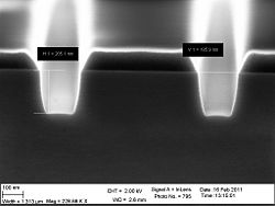
- The results of the Sinano3.2 recipe
-
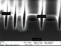 The 30 nm trenches
 -
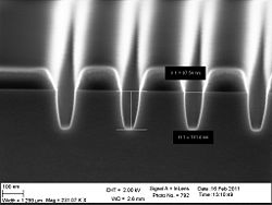 The 60 nm trenches
 -
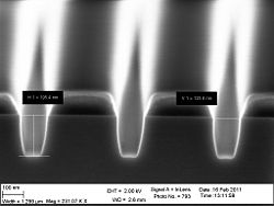 The 90 nm trenches
 -
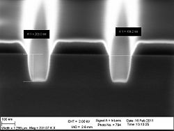 The 120 nm trenches
 -
 The 150 nm trenches


| Nominal trench line width | ' | ' | 30 | 60 | 90 | 120 | 150 | Average | Std. dev. |
| Etch rate | nm/min | 67 | 91 | 98 | 100 | 105 | 92 | 15 | |
| Sidewall angle | degs | 82 | 83 | 82 | 82 | 81 | 82 | 1 | |
| CD loss | nm/edge | -14 | -14 | -18 | -15 | -15 | -15 | 2 | |
| CD loss foot | nm/edge | -14 | -5 | -3 | 3 | 6 | -3 | 8 | |
| Bowing | 10 | 16 | 17 | 15 | 17 | 15 | 3 | ||
| Bottom curvature | -41 | -11 | -6 | 6 | 6 | -9 | 19 | ||
| Zep etch rate | 40 |