Specific Process Knowledge/Thin film deposition/Sputter coater: Difference between revisions
| Line 56: | Line 56: | ||
|- | |- | ||
|} | |} | ||
= The Balzer Sputter coater = | = The Balzer Sputter coater = | ||
| Line 84: | Line 85: | ||
!style="background:silver; color:black" align="left" valign="top" rowspan="2"|Performance | !style="background:silver; color:black" align="left" valign="top" rowspan="2"|Performance | ||
|style="background:LightGrey; color:black"|Film thickness||style="background:WhiteSmoke; color:black"| | |style="background:LightGrey; color:black"|Film thickness||style="background:WhiteSmoke; color:black"| | ||
*10 Å - | *10 Å - > 25 nm | ||
|- | |- | ||
|style="background:LightGrey; color:black"|Deposition rate | |style="background:LightGrey; color:black"|Deposition rate | ||
| Line 97: | Line 98: | ||
|style="background:LightGrey; color:black"|Process pressure | |style="background:LightGrey; color:black"|Process pressure | ||
|style="background:WhiteSmoke; color:black"| | |style="background:WhiteSmoke; color:black"| | ||
* | *2*10<sub> -2</sub> mbar | ||
|- | |- | ||
!style="background:silver; color:black" align="left" valign="top" rowspan="3"|Substrates | !style="background:silver; color:black" align="left" valign="top" rowspan="3"|Substrates | ||
|style="background:LightGrey; color:black"|Batch size | |style="background:LightGrey; color:black"|Batch size | ||
|style="background:WhiteSmoke; color:black"| | |style="background:WhiteSmoke; color:black"| | ||
*One 100 mm wafer | *One sample smaller than a 100 mm wafer | ||
*Several smaller samples | *Several smaller samples | ||
|- | |- | ||
Revision as of 15:54, 13 February 2014
Feedback to this page: click here
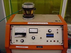
The Hummer Sputter coater
The Hummer sputter coater is used to sputter a thin gold layer on different small samples (up to 100 mm wafers).
One of the most effective ways to counter the problems with charging on non-conducting samples during SEM investigations is to apply a conducting coating to the surface. The Hummer sputter coater is an instrument that allows you to coat small samples with a gold layer. When securely grounded, i.e. connected electrically with a sample holder using aluminium tape or clamps the gold layer will effectively eliminate all charging problems in the SEM.
The Hummer sputter coater is located in servie area 3 in the clearoom.
The user manual and contact information can be found in LabManager:
Process knowledge
| Purpose |
| |
|---|---|---|
| Performance | Film thickness |
|
| Deposition rate |
| |
| Process parameter range | Process Temperature |
|
| Process pressure |
| |
| Substrates | Batch size |
|
| Allowed materials |
|
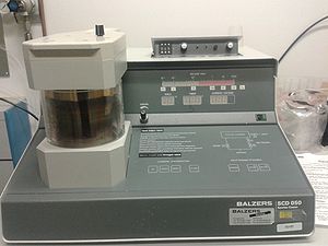
The Balzer Sputter coater
The Balzer sputter coater is used to sputter a thin gold layer on different small samples (smaller then 100 mm wafers).
One of the most effective ways to counter the problems with charging on non-conducting samples during SEM investigations is to apply a conducting coating to the surface. The Hummer sputter coater is an instrument that allows you to coat small samples with a gold layer. When securely grounded, i.e. connected electrically with a sample holder using aluminium tape or clamps the gold layer will effectively eliminate all charging problems in the SEM.
The Balzer sputter coater is located in the 346 basement, room 907 (next to the SEM Jeol) .
The user manual and contact information can be found in LabManager:
Process knowledge
| Purpose |
| |
|---|---|---|
| Performance | Film thickness |
|
| Deposition rate |
| |
| Process parameter range | Process Temperature |
|
| Process pressure |
| |
| Substrates | Batch size |
|
| Allowed materials |
|

