Specific Process Knowledge/Lithography/EBeamLithography/EBLProcessExamples: Difference between revisions
| (28 intermediate revisions by the same user not shown) | |||
| Line 9: | Line 9: | ||
The single shot approach is illustrated in the center and right parts of the figure below as there are two ways to go about this. | The single shot approach is illustrated in the center and right parts of the figure below as there are two ways to go about this. | ||
*''' | *'''Single big box approach''': This approach is illustrated in the center of the figure below. The mask is a single box of the desired size of the array. The beam is then pitched with the SHOT x, n command where n determines the beam pitch and hence the pitch of the resulting circles. The size of the resulting circles is determined by the dwell time. | ||
*''' | *'''Array of small boxes approach''': This is illustrated on the right side of the figure. In this approach each circle is represented by a small 2x2 nm box, hence the pattern is an array of these small boxes and the beam pitch is set higher than the size of the box to produce a single beam shot in each box. Again, the size of the resulting circles is determined by the dwell time. | ||
{| style="border: none; border-spacing: 0; margin: 1em auto; text-align: center;" | {| style="border: none; border-spacing: 0; margin: 1em auto; text-align: center;" | ||
| Line 21: | Line 21: | ||
|} | |} | ||
== | ==SHOT mode== | ||
For both of the single shot approaches the SHOT mode defined in the SDF file should be SHOT S, rather than the normal SHOT A. | |||
SHOT A mode is used with the RESIST command to define an area dose in µC/cm2 and the beam pitch in 1/4 nm steps. The following will for instance define an area dose of 300 µC/cm<big>2</big> and a beam pitch of 200 nm (800 x 1/4 nm): | |||
'''RESIST 300''' | |||
'''SHOT A, 800''' | |||
As the number of beam shots in a certain area scales with the shot pitch, the dwell time is in this way determined by the combination of area dose and beam pitch. If one changes the pitch, the dwell time and hence circle size will also change. One can decouple this relation by using SHOT S mode instead. In SHOT S mode the user defines the actual dwell time and hence in SHOT S mode the RESIST command is ignored. In SHOT S mode the user can thus define the dwell time and beam pitch independently. | |||
SHOT S takes three arguments as '''SHOT S, t1, t2, s''', where t1 is area dwell time in ns, t2 is line dwell time (not applicable to JEOL 9500) and s is shot pitch in 1/4 nm steps. The following example will set a dwell time of 550 ns and a beam pitch of 150 nm (600 x 1/4 nm): | |||
'''SHOT S, 550, 0, 600''' | |||
==Single big box approach== | |||
In this approach the mask is a single box determining the area of the array. The algorithm that places beam shots will seek to fill the shape as evenly as possible. Hence, the shot placements will not form an equidistant grid unless the size of the shape allows an integer number of beam shots to be placed in both axis. This is is illustrated below. To obtain a perfect grid the shot pitch must match both the subfield size and the total shape size, in the sense that an integer number of beam shots should be placed inside each subfield and an integer number of subfields should be placed inside the total shape. | |||
By default the subfield size is 4x4 µm. This will match for instance a beam pitch of 200 nm, since it will place 20 beam shots along each axis. It does not match a beam pitch of 190 nm for instance, since 4000 nm / 190 nm = 21.05. If one wants a beam pitch of 190 nm the subfield size should be changed to 3.990 x 3.990 µm. This is done in the JDF file by changing the '''SPPRM''' command from the usual '''SPPRM 4.0,,,,1.0,1''' to '''SPPRM 3.99,,,,1.0,1''', since the first number determines subfield size. | |||
A significant limitation of this approach is that the beam pitch as determined by the SHOT S command has a maximum value of 1020 units, i.e. 251 nm. The method described below does not have this limitation. | |||
{| style="border: none; border-spacing: 0; margin: 1em auto; text-align: center;" | |||
|- | |||
| [[Image:shot_placement.png|800px]] | |||
|- | |||
| colspan="1" style="text-align:center;| | |||
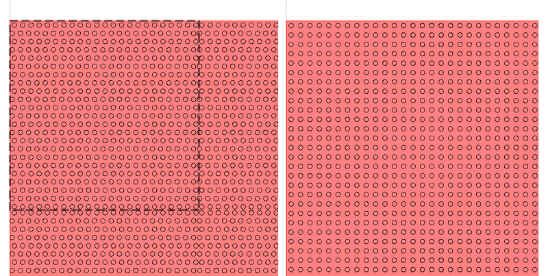
Example of shot placement. Left: The shot placement does not form an equidistant grid since the beam pitch does not fit an integer number of beam shots in the 4x4 µm subfield (indicated with dashed lines). Right: The beam pitch matches the subfield size and beam shots are placed in a perfect grid. | |||
|} | |||
==Array of small boxes approach== | |||
In this approach the pattern is an array of 2x2 nm boxes, each box will be filled with a single beam shot and hence the beam placement is determined by the boxes in the array. Thus, this is a more versatile approach as it allows the user to easily vary distance between shots and create hexagonal arrays or similar. The exposure is however somewhat slower since each shape adds a few ns of beam settling time. The beam pitch as setup in the SHOT S command should be large enough that a single beam shot is placed in each 2x2 nm box, i.e. it should just be larger than 2 nm. | |||
==Results== | ==Results== | ||
The results below are made with the approach described above. The pattern is defined in 180 nm AR-P 6200 on a silicon substrate, exposed at 29 nA. The circle size as a function of dwell time and beam pitch is illustrated in the graph. It is seen that the circle pitch has a significant impact on circle size even for the same dwell time, this is naturally due to the proximity effect and can not be avoided. The graph can however serve as a guide to chose the right combination of beam pitch and dwell time to obtain the array one desires. | |||
{| style="border: none; border-spacing: 0; margin: 1em auto; text-align: center;" | |||
|- | |||
| [[Image:SingleShotSEM.png|400px]] | |||
|- | |||
| colspan="1" style="text-align:center;| | |||
Example of circle array created with the single shot approach. | |||
|} | |||
{| style="border: none; border-spacing: 0; margin: 1em auto; text-align: center;" | {| style="border: none; border-spacing: 0; margin: 1em auto; text-align: center;" | ||
|- | |- | ||
| [[Image:SingleShotChart.png| | | [[Image:SingleShotChart.png|800px]] | ||
|- | |- | ||
| colspan="1" style="text-align:center;| | | colspan="1" style="text-align:center;| | ||
| Line 37: | Line 74: | ||
|} | |} | ||
You can read more about this method in the linked article. | |||
''' [http://www.sciencedirect.com/science/article/pii/S0167931714000987 Single-spot e-beam lithography for defining large arrays of nano-holes]''' | ''' [http://www.sciencedirect.com/science/article/pii/S0167931714000987 Single-spot e-beam lithography for defining large arrays of nano-holes]''' | ||
=Article on quality control on the JEOL 9500 system= | =Article on quality control on the JEOL 9500 system= | ||
''' [http://www.sciencedirect.com/science/article/pii/S0167931716300466 Quality control of JEOL JBX-9500FSZ lithography system in a multi-user laboratory]''' | ''' [http://www.sciencedirect.com/science/article/pii/S0167931716300466 Quality control of JEOL JBX-9500FSZ lithography system in a multi-user laboratory]''' | ||
Latest revision as of 09:53, 26 June 2024
This page is under construction. In time we will fill it with relevant process examples and relevant data.
Mix-and-match with EBL and UV lithography
Using mix-and-match it is possible to combine EBL and UV lithography using selected resists. Read more on the Mix-and-match page.
Circle arrays by single spot EBL on JEOL 9500
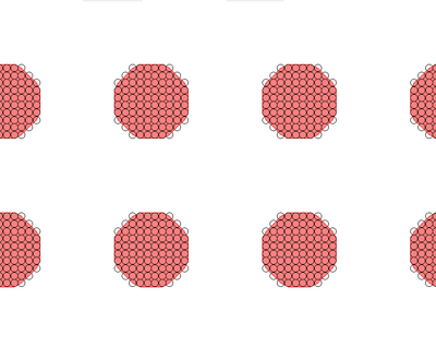
Arrays of circular holes can be created by normal area writing of a mask of circular structures, this is illustrated in the left side of the figure below. In this case the drawn circles are filled with beam shots, just like for any other area based exposure. For large arrays this can however be quite slow and hence it can be faster to write circles with local overexposure of single beam shots, i.e. a setup where the beam is pitched at the required circle pitch and the beam dwells at each site to produce a circle of the required size. In this approach dwell times will typically be in the order of several 100 ns to a few µs.
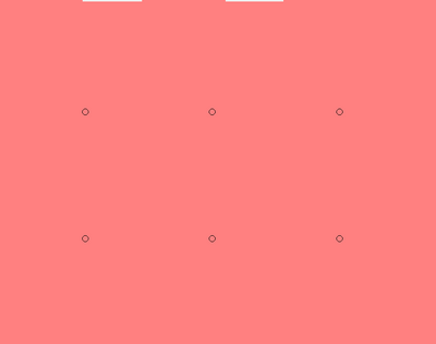
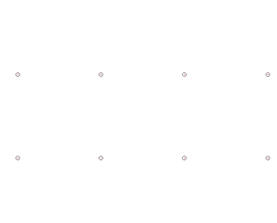
The single shot approach is illustrated in the center and right parts of the figure below as there are two ways to go about this.
- Single big box approach: This approach is illustrated in the center of the figure below. The mask is a single box of the desired size of the array. The beam is then pitched with the SHOT x, n command where n determines the beam pitch and hence the pitch of the resulting circles. The size of the resulting circles is determined by the dwell time.
- Array of small boxes approach: This is illustrated on the right side of the figure. In this approach each circle is represented by a small 2x2 nm box, hence the pattern is an array of these small boxes and the beam pitch is set higher than the size of the box to produce a single beam shot in each box. Again, the size of the resulting circles is determined by the dwell time.
 |
 |
|
|
Example of the three different approaches for exposing arrays of circles. In all cases the red areas are the areas drawn in the mask file. The small circles indicate beam positions. | ||
SHOT mode
For both of the single shot approaches the SHOT mode defined in the SDF file should be SHOT S, rather than the normal SHOT A.
SHOT A mode is used with the RESIST command to define an area dose in µC/cm2 and the beam pitch in 1/4 nm steps. The following will for instance define an area dose of 300 µC/cm2 and a beam pitch of 200 nm (800 x 1/4 nm):
RESIST 300
SHOT A, 800
As the number of beam shots in a certain area scales with the shot pitch, the dwell time is in this way determined by the combination of area dose and beam pitch. If one changes the pitch, the dwell time and hence circle size will also change. One can decouple this relation by using SHOT S mode instead. In SHOT S mode the user defines the actual dwell time and hence in SHOT S mode the RESIST command is ignored. In SHOT S mode the user can thus define the dwell time and beam pitch independently.
SHOT S takes three arguments as SHOT S, t1, t2, s, where t1 is area dwell time in ns, t2 is line dwell time (not applicable to JEOL 9500) and s is shot pitch in 1/4 nm steps. The following example will set a dwell time of 550 ns and a beam pitch of 150 nm (600 x 1/4 nm):
SHOT S, 550, 0, 600
Single big box approach
In this approach the mask is a single box determining the area of the array. The algorithm that places beam shots will seek to fill the shape as evenly as possible. Hence, the shot placements will not form an equidistant grid unless the size of the shape allows an integer number of beam shots to be placed in both axis. This is is illustrated below. To obtain a perfect grid the shot pitch must match both the subfield size and the total shape size, in the sense that an integer number of beam shots should be placed inside each subfield and an integer number of subfields should be placed inside the total shape.
By default the subfield size is 4x4 µm. This will match for instance a beam pitch of 200 nm, since it will place 20 beam shots along each axis. It does not match a beam pitch of 190 nm for instance, since 4000 nm / 190 nm = 21.05. If one wants a beam pitch of 190 nm the subfield size should be changed to 3.990 x 3.990 µm. This is done in the JDF file by changing the SPPRM command from the usual SPPRM 4.0,,,,1.0,1 to SPPRM 3.99,,,,1.0,1, since the first number determines subfield size.
A significant limitation of this approach is that the beam pitch as determined by the SHOT S command has a maximum value of 1020 units, i.e. 251 nm. The method described below does not have this limitation.
Array of small boxes approach
In this approach the pattern is an array of 2x2 nm boxes, each box will be filled with a single beam shot and hence the beam placement is determined by the boxes in the array. Thus, this is a more versatile approach as it allows the user to easily vary distance between shots and create hexagonal arrays or similar. The exposure is however somewhat slower since each shape adds a few ns of beam settling time. The beam pitch as setup in the SHOT S command should be large enough that a single beam shot is placed in each 2x2 nm box, i.e. it should just be larger than 2 nm.
Results
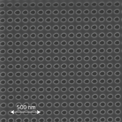
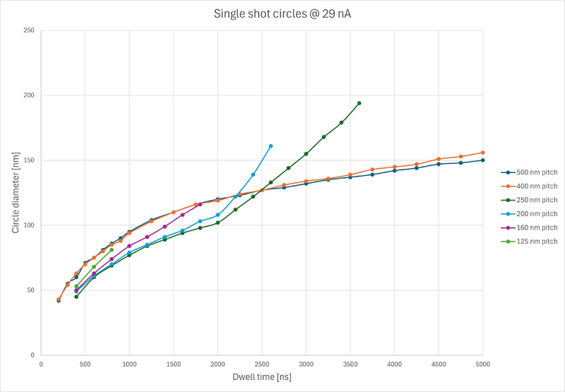
The results below are made with the approach described above. The pattern is defined in 180 nm AR-P 6200 on a silicon substrate, exposed at 29 nA. The circle size as a function of dwell time and beam pitch is illustrated in the graph. It is seen that the circle pitch has a significant impact on circle size even for the same dwell time, this is naturally due to the proximity effect and can not be avoided. The graph can however serve as a guide to chose the right combination of beam pitch and dwell time to obtain the array one desires.
|
|
Example of circle array created with the single shot approach. |
|
|
Circle size as a function of pitch and dwell time for exposure at 29 nA. |
You can read more about this method in the linked article.
Single-spot e-beam lithography for defining large arrays of nano-holes
Article on quality control on the JEOL 9500 system
Quality control of JEOL JBX-9500FSZ lithography system in a multi-user laboratory
