LabAdviser/314/Microscopy 314-307/SEM/QFEG
Feedback to this page: click here
This section is written by DTU Nanolab internal if nothing else is stated.
QFEG 200 Cryo ESEM (FEI Quanta FEG 200)
The QFEG 200 Cryo is an FEI Quanta FEG (Field Emission Gun) scanning electron microscope with a spatial resolution of 2 nm for the ETD detector in high vacuum at 30 keV. The microscope can operate in several modes, such as high vacuum, low vacuum, environmental mode, room temperature, low temperature and cryo. Our QFEG is fitted with an EDS detector, which allows for analytical measurements in all the operation modes. With the cryo transfer system available, it is especially suited for cryo experiments.
Process information
- Electron source
Field emission gun
- Accelerating voltage
500 V- 30 kV
- Resolution
2 nm at 30 kV (SE)
- Imaging detectors
Everhart-Thornley (SE/BSE), Solid State BSE, Large Field, Gaseous SE, Gaseous BSE, Gaseous Analytical, STEM, vCD and CCD Camera
- Imaging modes
High, low vacuum and environmental
- Analytical capabilities
Energy dispersive X-rays (Oxford Instruments 80 mm2 X-Max silicon drift detector, MnKα resolution at 124 eV)
- Attachments
Quorum PP2000 Cryo System, FEI Peltier stage (-10°C to 22°C).
| Equipment | QFEG Cryo SEM FEI Quanta FEG 200 | |
|---|---|---|
| Purpose | Vizualization and Microanalysis |
|
| Performance | Resolution | The resolution of QFEG dependends on the sample and the operation mode! |
| ||
| Instrument specifics | Detectors |
|
| Electron source |
| |
| Stage (room temperature) |
| |
| Peltier stage |
| |
| Cryo stage |
| |
| EDS |
| |
| Operating pressures |
| |
| Samples | Sample sizes |
|
| Allowed materials |
| |
Examples of the QFEG's capabilities
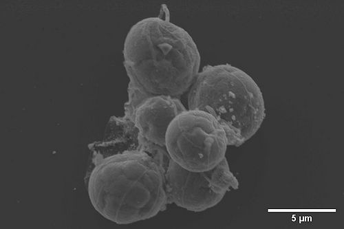
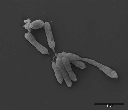
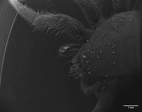
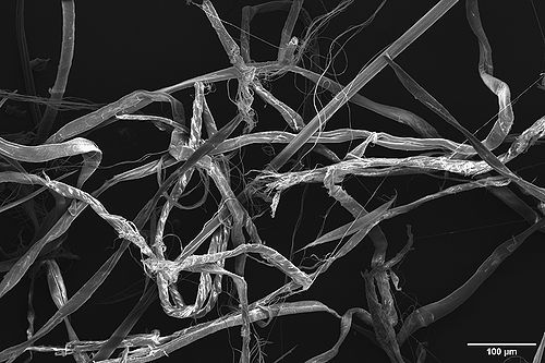
All images are taken by Marie Karen Tracy Hong Lin @DTU Nanolab
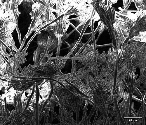
SEM (Scanning Electron Microscopy)
The SEM is a remarkable technique which can offer information such as the surface morphology of a sample and also a 3D appearance of the specimen. It can offer the best resolution (2 nm at 30kV) at high magnification and also topographical details because of its great depth of field.
BSD (Backscattered Electron Detector)
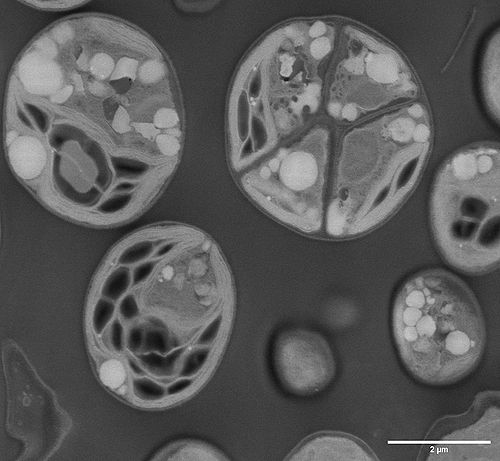
STEM (Scanning Transmission Electron Microscopy)
STEM combines the principles of transmission electron microscopy and scanning electron microscopy and can be performed on either type of instrument. In the STEM setting, the sample requires to have a thickness of less than 200 nm for visualization. Sample preparation prior to STEM microscopy involve samples being embedded in epoxy resin and then ultra sectioning using the Ultramicrotome. For more sensitive samples that need to be sectionned at cryogenic temperatures (below −180 °C), the Cryo-Ultramicrotome can be used for that purpose.
ESEM (Environmental Scanning Electron Microscopy)
In the ESEM setting, sample temperature and specimen chamber vapour pressure can both be controlled thus allowing visualiztion of the specimen when heated, cooled, wetted or dried.
Cryo-SEM
In the cryo-SEM setting, the sample is visualized in a frozen state (down to -190 °C). This setting is very useful when the specimen being observed needs visualiztion in its hydrated form. It can be imaged by using either the secondary electrons (SE) or backscattered electrons (BSE) detector.
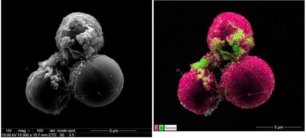
EDS (Energy Dispersive X-ray Spectroscopy)
The EDS is an analytical technique which can provide elemental or chemical characteristics of a sample.

