LabAdviser/Technology Research/Technology Development of 3D Silicon Plasma Etching process for Novel Devices and Applications
Feedback to this page: click here
Technology Development of 3D Silicon Plasma Etching process for Novel Devices and Applications
- Project type: Ph.d. project
- Project responsible: Bingdong Chang
- Supervisors:Henri Jansen, Flemming Jensen, Jörg Hübner
- Partners involved: DTU Danchip
- Full Thesis: https://orbit.dtu.dk/en/publications/technology-development-of-3d-silicon-plasma-etching-processes-for
Project Description
Plasma processes are important for silicon-based micro electromechanical systems (MEMS) with critical dimensions around a few microns. With the lithographic tools pushing the limits further down, also the dimensions of MEMS devices are rapidly decreasing and commercial nano electromechanical systems (NEMS) are underway. Emerging applications include NEMS resonators and sensors for physical and bio-chemical sensing down to the molecular level both because of the much reduced mass, nanowires for novel transistors and photovoltaics increasingly exploring quantum effects starting at the sub-50nm level, nanostructures for photonics (around the wavelength of the guided photons) and next generation storage (10nm and below), black silicon for large area catalysed reaction chambers and photovoltaics, through wafer vias for packaging applications, and nano imprint lithography (NIL) masters. Furthermore, instead of silicon, diamond is increasingly important as a structural material because of its remarkable properties such as electrical conductivity and hardness.
Typically all these devices have customized process flows but synergies can be found as most are produced using a 2.5D approach comprising sequential deposition, lithography and etch steps. The majority, such as accelerometers and gyroscopes, are based on sub-100 micron depth features with piezo-resistive transduction or submicron gap capacitive sensing. Trends are towards higher aspect ratio etches (depth/width>30) and small footprint devices for enhanced performance. Increasingly, large cavities (10-100 microns in width) are being etched for subsequent chip or wafer scale packaging and sensor structures may comprise multi-wafer stacks with one or more having through wafer etches (200-800 microns deep). High speed etching with excellent profiles control to facilitate e.g. copper feedthroughs is indispensable for such applications. For NIL applications, it is essential that the mold releases cleanly and a smooth sidewall without any negative profile that would prevent release.
Although widely utilized and largely understood, silicon etch processes fail to reproduce at the nanoscale. Transport effects ‘down the etched cavity’ limit rate and selectivity while aspect ratios, profile and passivation control are more challenging. For example, aspect ratios beyond 30 are rarely utilized and fluctuations in the results are common. So, at the nanoscale, etching becomes more difficult. Basically, two types of etching techniques can be distinguished; the continuous (or mixed) process and the alternating (or pulsed/Bosch) process. The continuous process generally has smooth sidewalls and low undercut and it is the standard technique in mainstream nano-electronic chip fabrication. However, at room temperature the mixed gas process, results in a low rate selectivity and aspect ratio capability – as such it is limited to shallow features. The alternating etch process is probably the most popular technique in MEMS production facilities today. It uses a repeating sequence of plasma enhanced deposition to passivate silicon features, a physical etch for directional removal of this layer at the base of the features, and an isotropic etch for silicon removal at the cleared surfaces. However, it is not well suited to the nanoscale due to finite sidewall scallop size and undercut unless rate and selectivity are severely compromised. Typically it is not applied below 500nm trench feature sizes – although 100nm features have been demonstrated.
The major part of this project will be related to experimental work in the cleanroom facility at DTU Danchip. It is the quest to develop a fundamental understanding of the special challenges involved in dry etching at the nanoscale including the physics and chemistry involved in the processing. The aim is to establish a generic knowledge platform for the nanoscale dry etching for future applications. An important part of the project will be to demonstrate the ability of 3D plasma etching technology in both micro- and nanoscale.
Firstly, the applications of 3D silicon structures will be explored for nanophotonics study, e.g. deep subwavelength scattering of silicon nanostructures and photonic crystals, or photonic bandgap (PBG) structures. Since previous studies are mostly focused in 1D or 2D structures, e.g. planar waveguides, distributed Bragg reflectors, etc, while 3D structures can provide possibility to control and manipulate light in all three spatial dimensions. The fabrication of 3D silicon nanostructures, however, is difficult with traditional techniques and the structure quality is limited. In this study, 3D silicon nanostructures (e.g. vertically stacked silicon nanowires, 3D silicon simple cubic structures) will be fabricated and the optical properties will be characterized.
Secondly, 3D silicon structures will be combined with other functional materials, and the applications (e.g. photocurrent generation and photocatalysis) will be demonstrated. Since silicon has been studied extensively in the traditional semiconductor industry, in order to realize some novel applications and devices, a widely used method is to integrate other materials with silicon to form heterostructures, e.g. with zinc oxide, zinc sulphide, etc. With 3D engineered silicon, the device performance can be enhanced due to its increased surface area, and the substrate can be used repeatedly with a stable property. In this project, zinc oxide and metal organic frameworks structures will be integrated with microscale silicon structures, and the photocatalytic and photoelectric properties will be studied.
For this, a modern e-beam lithography tool will be utilized to define the NEMS structure down to 10nm critical dimension on top of a silicon on insulator (SOI) wafer. Subsequently, the pattern is transferred into the silicon layer using a modern high-density plasma tool. Finally, for certain applications the NEMS structure has to be released using isotropic undercutting of the oxide. If time permits the processing will be extended to diamond and diamond on insulator films.
Publications in peer-reviewed journal papers
The results achieved during the ph.d. project have been published on some peer-reviewed journals, which are listed as below:
Publications as first author
- DREM: Infinite etch selectivity and optimized scallop size distribution with conventional photoresists in an adapted multiplexed Bosch DRIE process
- Chang, B., Leussink, P., Jensen, F., Hübner, J. and Jansen, H.,
- Microelectronic Engineering, 191, pp.77-83 (2018) DOI
- DREM2: a facile fabrication strategy for freestanding three dimensional silicon micro-and nanostructures by a modified Bosch etch process
- Chang, B., Jensen, F., Hübner, J. and Jansen, H
- Journal of Micromechanics and Microengineering, 28(10), p.105012 (2018) DOI
- Confined Growth of ZIF‐8 Nanocrystals with Tunable Structural Colors
- Chang, B., Yang, Y., Jansen, H., Ding, F., Mølhave, K. and Sun, H.
- Advanced Materials Interfaces, 5(9), p.1701270 (2018) DOI
- Highly Ordered 3D Silicon Micro‐Mesh Structures Integrated with Nanowire Arrays: A Multifunctional Platform for Photodegradation, Photocurrent Generation, and Materials Conversion
- Chang, B., Tang, Y., Liang, M., Jansen, H., Jensen, F., Wang, B., Mølhave, K., Hübner, J. and Sun, H.
- ChemNanoMat (2018) DOI
- Large Area Three- Dimensional Photonic Crystal Membranes: Single-Run Fabrication and Applications with Embedded Planar Defects
- Chang, B., Zhou, C., Tarekegne, A., Yang, Y., Zhao, D., Jensen, F., Hübner, J., Jansen, H.
- Advanced Optical Materials (2018) DOI
Publications as co-author
- Inductively coupled plasma nanoetching of atomic layer deposition alumina
- Han, A., Chang, B., Todeschini, M., Le, H. T., Tiddi, W., and Keil, M.
- Microelectronic Engineering (2018) DOI
Conference contributions
The results achieved during the ph.d. project have been presented in the following conferences.
- RIE-lag “Correction” and Infinite Etching Selectivity with Conventional Photoresist in a Bosch Process
- Chang, B., Leussink, P., Jensen, F., Hübner, J. and Jansen, H.
- Poster presentation at 43rd International conference on Micro and Nano Engineering, Braga, Portugal (2017)
- Three dimensional engineering of silicon micro- and nanostructures
- Chang, B., Jensen, F., Hübner, J. and Jansen, H.
- Oral presentation at 44rd International conference on Micro and Nano Engineering, Copenhagen, Denmark (2018)
Student projects
During the ph.d. projects, following student projects have been offered for bachelor students. The final student reports can be found in the cleanroom drive: (O:\CleanroomDrive\bincha\3 week courses)
- High Resolution Pattern Definition with Electron Beam Lithography
- Mikro 3W, course no. 33470 (June 2016)
- Precise Timing Control in Deep Reactive Ion Etching (DRIE) with Bosch Process
- Mikro 3W, course no. 33470 (January 2017)
- Using the Black Silicon Method to Monitor the Reproducibility of Plasma Etching Processes
- Mikro 3W, course no. 33470 (July 2017)
Relevant technology details
Several fabrication technologies have been developed and optimized during the ph.d. project, which are listed as below.
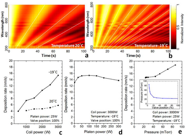
Plasma etching process have been performed mostly on the DRIE-Pegasus system. High aspect ratio structures, 3D structures and black silicon have been fabricated, technology details are accessible in the following pages:
- Etch high aspect ratio silicon microstructures
- Etch 3 dimensional silicon microstructures
- Etch black silicon
- Using OES to monitor etch process
For high resolution nanostructure patterning, electron beam writer JEOL_JBX-9500FSZ has been used with HSQ as a high resolution e-beam resist, technology details are accessible in the following page:
Galleries
Below are images illustrating works that have been done during the ph.d. projects.
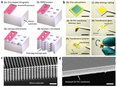
1. 3D silicon photonic crystal membranes.

2. Comparison of scallops by traditional Bosch process and modified DREM process.
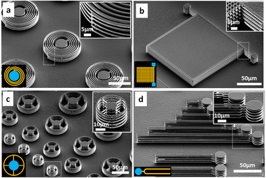
3. 3D silicon microstructures fabricated by DREM process.
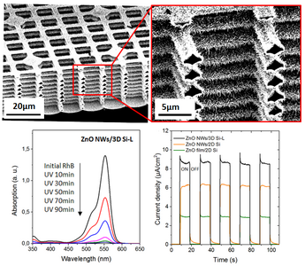
4. 3D silicon micro-mesh structures integrated with ZnO nanowires for photocatalysis and photocurrent generation.

5. 3D silicon stacked nanowires for structural color generation.
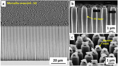
6. High aspect ratio silicon micropillars fabricated with DREM process.
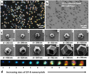
7. ZIF-8 crystals for tunable structural colors.
8. Using OES to monitor the fluorocarbon film deposition with Pegasus 1.


