Specific Process Knowledge/Etch/DRIE-Pegasus/Etch high aspect ratio silicon microstructures
Feedback to this page: click here
By performing a finely tuned process, which is called DREM process (Deposit, Removal, Etch Method), an infinite etch selectivity can be achieved with conventional photoresist, and in the same time, the scallop size is almost identical from top to the bottom of the etch profile. This gives possibility for etching high aspect ratio silicon structures, and an aspect ratio of more than 50 has been demonstrated for trench structures (1µm linewidth with 10µm pitch) and pillar structures (1µm diameter, 2µm pitch in triangular lattice).
Unlike traditional Bosch process, DREM process consists of 3 finely tuned steps (deposit, bottom removal and etch), in which the first two step: deposit and bottom removal are carefully tuned to be balanced, this means that during every cycle, the bottom of the trench is clean from fluorocarbon deposition, while on top of the resist, there is still some residue of fluorocarbon layer that can protect the mask from being attacked, thus the DREM process can continue without consuming any mask materials. In the same time, the etch duration ramps up when DREM process continues, which can compensate for the etch non uniformity caused by RIE-lag, and a uniform scallop size distribution can be achieved.
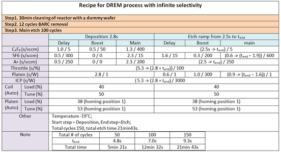
A complete recipe is shown as below:
- Parameter settings for a DREM process recipe on DRIE-Pegasus

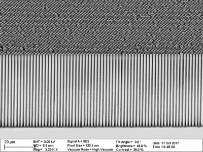
Below are some SEM images of the high aspect silicon nanostructures achieved by DREM process:
- Silicon micropillars with aspect ratio of more than 50
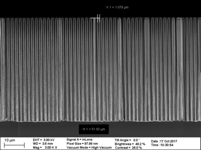


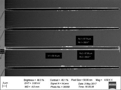
- Silicon microtrenches with aspect ratio of more than 50
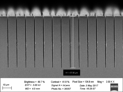


DUV lithography was used to define the patterns for the structures above (with 750nm thick KRF M230Y positive resist). The trench structures were achieved with DUV resist as etch mask, while the pillar structures were etched with 50nm alumina as a hard mask (the alumina mask can be etched by metal ICP).
For more details, please contact Henri Jansen (henrija@dtu.dk) or Bingdong Chang (bincha@dtu.dk)