|
|
| Line 295: |
Line 295: |
| =Etch test of Silicon Nitride= | | =Etch test of Silicon Nitride= |
|
| |
|
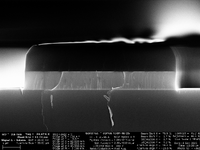
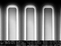
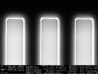
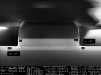
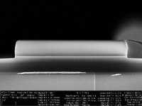
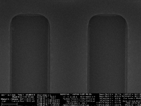
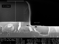
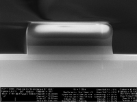
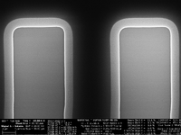
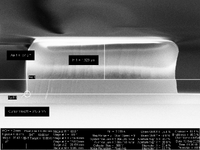
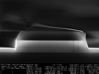
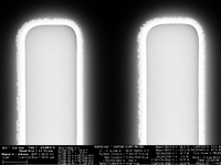
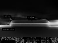
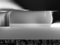
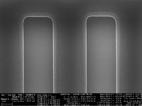
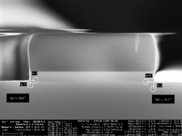
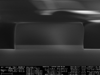
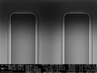
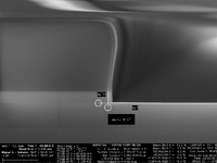
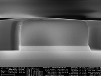
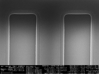
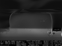
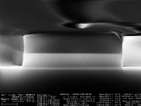
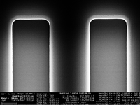
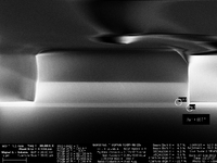
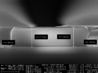
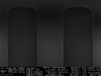
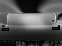
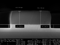
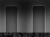
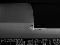
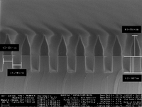
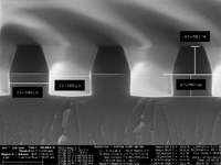
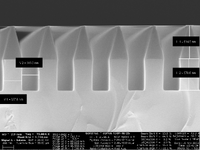
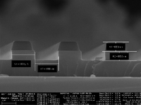
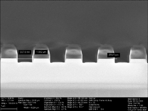
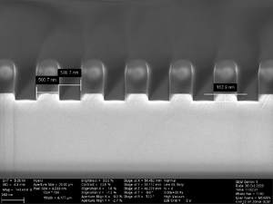
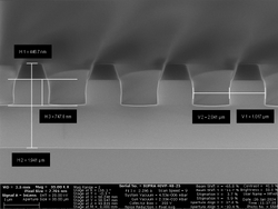
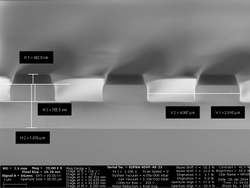
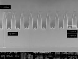
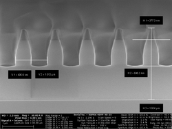
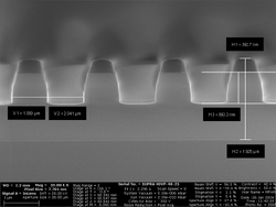
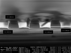
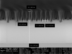
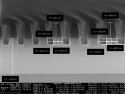
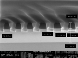
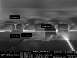
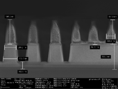
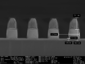
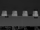
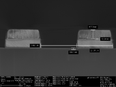
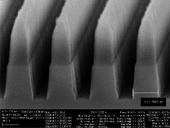
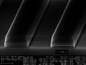
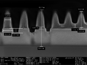
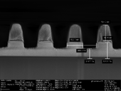
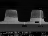
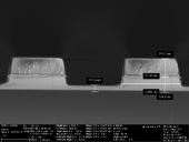
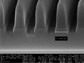
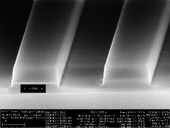
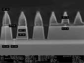
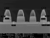
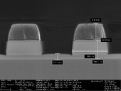
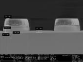
| Tested on chips (2*2cm). The following results were processed on chips bonded to a 100mm dummy wafer. They were patterned with 750 DUV resist and 65nm of BARC (exposure:355 J/m2, focus:-3.1). The nitride layer was 560nm, deposited on the PECVD4 (Standard HF SiN with wafer clean).
| | The nitride layer deposited was 560nm, on the PECVD4 (recipe: Standard HF SiN with wafer clean, for 1h). |
| | | They were patterned with 750 DUV resist and 65nm of BARC (exposure:355 J/m2, focus:-3.1). |
| | The following results were processed on chips (2*2cm) bonded to a 100mm dummy wafer. |
|
| |
|
|
| |
|
Revision as of 14:57, 22 April 2024
Tests performed with UV resist:
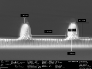
The tests were performed on a 100mm wafer patterned on MLA3, with 2.2um AZ5214E resist.
| Recipe
|
Recipe parameters
|
Duration (min)
|
Date
|
SEM picture
|
Redeposition - top view
|
Profile angles
|
Etch rate in SiO2
|
Etch rate in resist
(AZ5214E inverse)
|
Selectivity
(SiO2:resist)
|
| CHF3_t1
|
CHF3= 22.5 sccm
Coil= 800W
Platen= 15W
Press= 2.5mTorr
Temp= 20°C
|
12:00
|
04/09/2023
|

|

|
|
69.7 nm/min
+/- 10.5%
|
57.3 nm/min
+/- 12.9%
|
1.22
|
| CHF3_t2
|
CHF3= 22.5 sccm
Coil= 150W
Platen= 25W
Press= 2.5mTorr
Temp= 20°C
|
25:00
|
04/09/2023
|

|

|

|
26.7 nm/min
+/- 11.9%
|
24.2 nm/min
+/- 21.1%
|
1.1
|
| CHF3 t2
|
CHF3= 22.5 sccm
H2= 22.5 sccm
Coil= 150W
Platen= 25W
Press= 2.5mTorr
Temp= 20°C
|
10:00
|
22/09/2023
|

|

|

|
9,7 nm/min
+/- 34.4%
|
1,8 nm/min
+/- 46.5%
|
5.4
|
| CHF3_t1
|
CHF3= 22.5 sccm
H2= 10 sccm
Coil= 800W
Platen= 15W
Press= 2.5mTorr
Temp= 20°C
|
10:00
|
12/09/2023
|

|

|

|
59,6 nm/min
+/- 12.9%
|
47,5 nm/min
+/- 21.5%
|
1.25
|
| CHF3_t1
|
CHF3= 22.5 sccm
O2= 10 sccm
Coil= 800W
Platen= 15W
Press= 2.5mTorr
Temp= 20°C
|
10:00
|
11/09/2023
|

|

|

|
60,6 nm/min
+/- 10.1%
|
130,8 nm/min
+/- 8.8%
|
0.46
|
| CHF3 t1
|
CHF3= 22.5 sccm
H2= 22.5 sccm
Coil= 800W
Platen= 15W
Press= 2.5mTorr
Temp= 20°C
|
10:00
|
20/09/2023
|

|

|

|
47,3 nm/min
+/- 12%
|
26,4 nm/min
+/- 17,4%
|
1.8
|
| CHF3 t1
|
CHF3= 22.5 sccm
H2= 35 sccm
Coil= 800W
Platen= 15W
Press= 2.5mTorr
Temp= 20°C
|
10:00
|
22/09/2023
|

|

|

|
36,5 nm/min
+/- 10.6%
|
17,5 nm/min
+/- 13.9%
|
2.09
|
| CHF3 t1
|
CHF3= 35 sccm
H2= 35 sccm
Coil= 800W
Platen= 15W
Press= 2.5mTorr
Temp= 20°C
|
10:00
|
22/09/2023
|

|

|

|
42 nm/min
+/- 15.4%
|
23,8 nm/min
+/- 22.2%
|
1.76
|
| CHF3 t1
|
CHF3= 22.5 sccm
CF4= 22.5 sccm
Coil= 800W
Platen= 15W
Press= 2.5mTorr
Temp= 20°C
|
10:00
|
22/09/2023
|

|

|

|
75,8 nm/min
+/- 13.1%
|
74,9 nm/min
+/- 10.8%
|
1.01
|
| CHF3 t1
|
CHF3= 22.5 sccm
H2= 22.5 sccm
Coil= 800W
Platen= 15W
Press= 25mTorr
Temp= 20°C
|
10:00
|
22/09/2023
|

|

|

|
-
|
-
|
no etch done,
polymer deposited
|
| CHF3 t1
|
CHF3= 22.5 sccm
H2= 22.5 sccm
Coil= 800W
Platen= 15W
Press= 2.5mTorr
Temp= 0°C
|
10:00
|
22/09/2023
|

|

|

|
48 nm/min
+/- 11.2%
|
23,3 nm/min
+/- 13.7%
|
2.06
|
Tests performed with DUV resist:
The resist used was a negative DUV resist (UVN) with 915nm + 88nm BARC layer.
| Recipe
|
Recipe parameters
|
Duration (min)
|
Date
|
SEM picture
|
Etch rate in SiO2
|
Etch rate in resist
(UVN)
|
Selectivity
(SiO2:resist)
|
| CHF3_t1
|
CHF3= 22.5 sccm
H2= 22.5 sccm
Coil= 800W
Platen= 30W
Press= 2.5mTorr
Temp= 20°C
|
10:00
|
13/11/23
|
 
|
47
|
24.6
|
1.9
|
| CHF3_t1
|
CHF3= 22.5 sccm
H2= 22.5 sccm
Coil= 800W
Platen= 45W
Press= 2.5mTorr
Temp= 20°C
|
10:00
|
13/11/23
|
 
|
59
|
30
|
1.9
|
| CHF3_t1
|
CHF3= 22.5 sccm
H2= 22.5 sccm
Coil= 800W
Platen= 45W
Press= 2.5mTorr
Temp= 0°C
|
10:00
|
07/12/23
|

|
96
|
56
|
1.7
|
| CHF3_t2
|
CHF3= 22.5 sccm
H2= 22.5 sccm
Coil= 150W
Platen= 25W
Press= 2.5mTorr
Temp= 20°C
|
10:00
|
23/10/23
|

|
27
|
12,5
|
2.1
|
| CHF3_t2
|
CHF3= 22.5 sccm
H2= 22.5 sccm
Coil= 150W
Platen= 25W
Press= 2.5mTorr
Temp= 20°C
|
20:00
|
23/10/23
|

|
8.15
|
7.5
|
1.1
|
2SiO2 test - 5 jan 2024
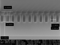
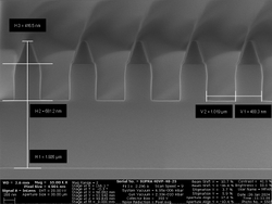
Tested on chips (2*2cm). The following results were processed on chips bonded to a 100mm wafer. They were patterned with 915 UVN resist (DUV negative) and 65nm of BARC. The SiO2 layer was 2um (deposited on the C1 furnace).
| Recipe
|
Time (min)
|
Date
|
SEM picture
|
Etch rate SiN (nm/min)
|
Etch rate resist (nm/min)
|
Selectivity
(SiN:resist)
|
CHF3_t1
CHF3= 22.5 sccm
H2= 22.5 sccm
Coil= 800W
Platen= 30W
Press= 2.5mTorr
Temp= 20°C
|
10:00
|
25/01
-2024
|
   
|
250nm- 61,99
500nm- 68,12
1000nm- 74,7
2000nm- 76,55
|
250nm- 61,31
500nm- 49,85
1000nm- 46,83
2000nm- 47,3
|
250nm- 1,01
500nm- 1,37
1000nm- 1,6
2000nm- 1,62
|
CHF3_t1
CHF3= 22.5 sccm
H2= 22.5 sccm
Coil= 150W
Platen= 45W
Press= 2.5mTorr
Temp= 20°C
|
10:00
|
25/01
-2024
|
   
|
250nm- 90,74
500nm- 84,63
1000nm- 89,33
2000nm- 94,34
|
250nm- 81,1
500nm- 53,77
1000nm- 52,23
2000nm- 54,81
|
250nm- 1,12
500nm- 1,57
1000nm- 1,71
2000nm- 1,72
|
CHF3_t2
CF4= 22.5 sccm
H2= 22.5 sccm
Coil= 150W
Platen= 45W
Press= 2.5mTorr
Temp= 20°C
|
15:00
|
25/01
-2024
|
   
*it's visible that redeposits, so the ER and selectivity may not be correct.
|
250nm- 9,18
500nm- 22,46
1000nm- 28,03
2000nm- 28,75
|
250nm- 11,09
500nm- 3,96
1000nm- 4,22
2000nm- 4,40
|
250nm- 0,83
500nm- 5,67
1000nm- 6,64
2000nm- 6,5
|
Etch test of Silicon Nitride
The nitride layer deposited was 560nm, on the PECVD4 (recipe: Standard HF SiN with wafer clean, for 1h).
They were patterned with 750 DUV resist and 65nm of BARC (exposure:355 J/m2, focus:-3.1).
The following results were processed on chips (2*2cm) bonded to a 100mm dummy wafer.
| Recipe
|
Time (min)
|
Date
|
SEM picture
|
Redeposition - top view
|
Etch rate SiN (nm/min)
|
Etch rate resist (nm/min)
|
Selectivity
(SiN:resist)
|
CHF3_t1
CHF3= 22.5 sccm
H2= 22.5 sccm
Coil= 800W
Platen= 15W
Press= 2.5mTorr
Temp= 20°C
|
2:30
|
29/02
-2024
|
   
|
 
|
250nm- 155,08
500nm- 170,32
1000nm- 174,45
2000nm- 179,76
|
250nm- 65,52
500nm- 56,36
1000nm- 64,56
2000nm- 68,84
|
250nm- 2,37
500nm- 3,02
1000nm- 2,70
2000nm- 2,61
|
CHF3_t2
CHF3= 22.5 sccm
H2= 22.5 sccm
Coil= 150W
Platen= 45W
Press= 2.5mTorr
Temp= 20°C
|
5:00
|
29/02
-2024
|
   
|
 
|
250nm- 28,12
500nm- 41,86
1000nm- 66
2000nm- 63,62
|
250nm- 23,26
500nm- 22,60
1000nm- 16,74
2000nm- 15,34
|
250nm- 1.21
500nm- 1.85
1000nm- 3.94
2000nm- 4.15
|
CF4lowCP
CF4= 22.5 sccm
H2= 22.5 sccm
Coil= 150W
Platen= 45W
Press= 2.5mTorr
Temp= 20°C
|
5:00
|
29/02
-2024
|
   
|
 
|
250nm- 76,50
500nm- 73,92
1000nm- 73,94
2000nm- 76,50
|
250nm- 44,98
500nm- 33,52
1000nm- 31,16
2000nm- 25,66
|
250nm- 1,70
500nm- 2,21
1000nm- 2,37
2000nm- 2,98
|
