|
|
| Line 215: |
Line 215: |
| <br> | | <br> |
|
| |
|
| ===Recipes and results - <span style="background:#FFD850">CF<sub>4</sub> / H<sub>2</sub> tests</span> === | | ===Recent results - <span style="background:#FFD850">CF<sub>4</sub> / H<sub>2</sub> tests</span> === |
|
| |
|
| The following results were processed on chips bonded to a 100mm wafer. They were patterned with 915 UVN resist (DUV negative) and 65nm of BARC. The SiO2 layer was 2um (deposited on the C1 furnace). | | The following results were processed on chips bonded to a 100mm wafer. They were patterned with 915 UVN resist (DUV negative) and 65nm of BARC. The SiO2 layer was 2um (deposited on the C1 furnace). |
Revision as of 14:03, 22 April 2024
More test with CF4/H2 - SiO2 etch
Tests performed by Maria Farinha @DTU Nanolab
The gas flows were combined and the following results were achieved. It´s visible that with higher CF4 the selectivity is not good, so by adding H2, until 1:1, the selectivity improves. Additionally, the uniformity gets slightly worse while going for 1:1 of gas chemistry.
The recipe CF4lowCP 22.5/22.5 seems to be the only one good enough to use. It is a slow etch recipe, with good selectivity with AZ5214E resist.
| CF4ICP
|
SiO2 ER (nm/min)
|
Uniformity (SiO2 etch)
|
Selectivity (SiO2:resist)
|
Si3N4 ER (nm/min)
|
SixN ER (nm/min)
|
| 45 CF4 + 0 H2
|
71.4
|
11.7%
|
0.74
|
-
|
-
|
| 35 CF4 + 10 H2
|
69
|
12.6%
|
0.89
|
-
|
-
|
| 22.5 CF4 + 22.5 H2
|
58.6
|
13.3%
|
1.43
|
84.4
|
42.9
|
- The uniformity considers a 100mm wafer, calculated with 5 points.
| CF4lowCP
|
SiO2 ER (nm/min)
|
Uniformity (SiO2 etch)
|
Selectivity (SiO2:resist)
|
Si3N4 ER (nm/min)
|
SixN ER (nm/min)
|
| 45 CF4 + 0 H2
|
24.9
|
11.5%
|
0.47
|
-
|
-
|
| 35 CF4 + 10 H2
|
22.6
|
11.6%
|
0.64
|
-
|
-
|
| 22.5 CF4 + 22.5 H2
|
17.8
|
13.7%
|
1.85
|
28
|
22.5
|
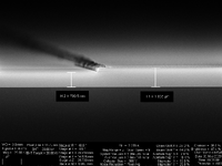
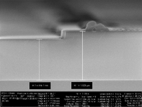
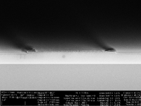
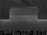
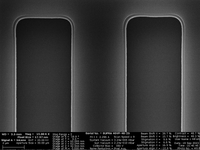
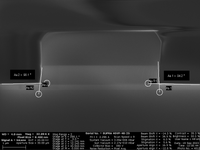
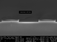
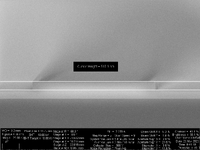
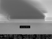
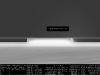
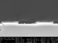
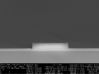
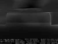
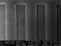
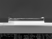
Profile pictures of some tests - April 2023
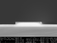
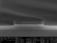
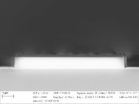
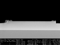
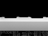
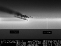
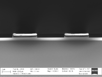
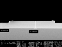
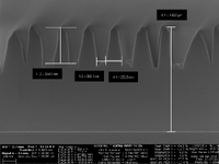
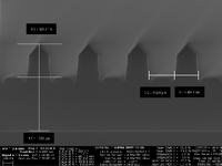
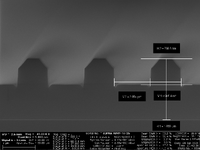
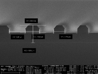
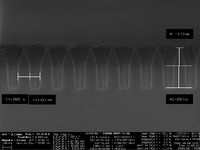
Even in the cases with the resist strip (plasma asher 2 processing for 10/15min), there are some traces of resist left on the edges of the features.
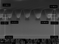
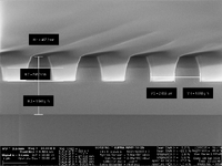
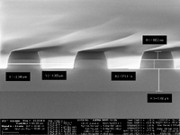
Also, it´s noticeable that the feature profile is trenching, being more evident with faster etch rates.
| CF4ICP 45 CF4 + resist strip
|
CF4ICP 45 CF4 / 10 H2 + resist strip
|
CF4ICP 35 CF4/ 10 H2
|
CF4lowCP 45 CF4/ 10 H2
|
CF4lowCP 45 CF4/ 0 H2 + resist strip
|
CF4lowCP 35 CF4/ 10 H2 + resist strip
|
CF4lowCP 22.5 CF4/ 22.5 H2 + resist strip
|

|

|

|

|
 
|
 
|
 
|
Recipes and results - CF4 / H2 tests
| Recipe
|
Recipe parameters
|
Process time
|
Date
|
SEM picture
|
Etch rate in SiO2
|
Etch rate in resist
(AZ5214E inverse)
|
Selectivity
(SiO2:resist)
|
| CF4ICP 22.5/22.5
|
CF4= 22.5 sccm
H2= 22.5 sccm
Coil= 800W
Platen= 15W
Press= 2.5mTorr
Temp= 20°C
|
11:00 min
|
11/09/2023
|
  
|
68 nm/min
+/- 8.5%
|
60,2 nm/min
+/- 9%
|
1.13
|
| CF4ICP 35/10
|
CF4= 35 sccm
H2= 10 sccm
Coil= 800W
Platen= 15W
Press= 2.5mTorr
Temp= 20°C
|
08:00 min
|
March 2023
|
 
|
69 nm/min
+/- 11.1%
|
77,1 nm/min
+/- 9.4%
|
0.9
|
| CF4ICP 45/0
|
CF4= 45 sccm
H2= 0 sccm
Coil= 800W
Platen= 15W
Press= 2.5mTorr
Temp= 20°C
|
08:00 min
|
March 2023
|
 
|
71.4 nm/min
+/- 10.3%
|
96,5 nm/min
+/- 6.0%
|
0.74
|
| CF4ICP 45/10
|
CF4= 45 sccm
H2= 10 sccm
Coil= 800W
Platen= 15W
Press= 2.5mTorr
Temp= 20°C
|
08:00 min
|
March 2023
|
 
|
67.8 nm/min
+/- 14.9%
|
88,86 nm/min
+/- 4.8%
|
0.76
|
| CF4lowCP 22.5/22.5
|
CF4= 22.5 sccm
H2= 22.5 sccm
Coil= 150W
Platen= 25W
Press= 2.5mTorr
Temp= 20°C
|
20:00 min
|
Sept 2023
|
 
|
23.8 nm/min
+/- 11%
|
20,6 nm/min
+/- 19.4%
|
1.16
|
| CF4lowCP 35/10
|
CF4= 35 sccm
H2= 10 sccm
Coil= 150W
Platen= 25W
Press= 2.5mTorr
Temp= 20°C
|
10:00 min
|
Feb 2023
|
 
|
22.65 nm/min
+/- 10.2%
|
35.9 nm/min
+/- 10.1%
|
0.63
|
| CF4lowCP 45/0
|
CF4= 45 sccm
H2= 0 sccm
Coil= 150W
Platen= 25W
Press= 2.5mTorr
Temp= 20°C
|
10:00 min
|
Feb 2023
|
 
|
24.9 nm/min
+/- 10.1%
|
52,3 nm/min
+/- 7.1%
|
0.47
|
| CF4lowCP 45/10
|
CF4= 45 sccm
H2= 10 sccm
Coil= 150W
Platen= 25W
Press= 2.5mTorr
Temp= 20°C
|
10:00 min
|
Feb 2023
|

|
29,4 nm/min
+/- 13.7%
|
100,6 nm/min
+/- 16.5%
|
0.29
|
Recent results - CF4 / H2 tests
The following results were processed on chips bonded to a 100mm wafer. They were patterned with 915 UVN resist (DUV negative) and 65nm of BARC. The SiO2 layer was 2um (deposited on the C1 furnace).
| CF4ICP @ 30W platen, 8min
|
| Values
|
SEM pictures
|
Comments
|
| Structure size (nm)
|
structure pitch (nm)
|
SiO2 ER (nm/min)
|
Resist ER (nm/min)
|
Selectivity SiO2/resist
|
|
|
| 250
|
500
|
69.36
|
114.38
|
0.61
|

|
Across the sample, the resist was fully etched away
|
| 500
|
1000
|
87.04
|
114.38
|
0.76
|

|
|
| 1000
|
2000
|
98.83
|
114.38
|
0.86
|

|
|
| 2000
|
4000
|
100.03
|
114.38
|
0.87
|

|
|
| CF4lowCP @ 45W platen, 15min
|
| Values
|
SEM pictures
|
Comments
|
| Structure size (nm)
|
structure pitch (nm)
|
SiO2 ER (nm/min)
|
Resist ER (nm/min)
|
Selectivity SiO2/resist
|
|
|
| 250
|
500
|
33.54
|
33.45
|
1.0
|

|
there was visible redeposition across smaller structures
|
| 500
|
1000
|
35.94
|
30.45
|
1.18
|

|
|
| 1000
|
2000
|
36.54
|
29.85
|
1.22
|

|
|
| 2000
|
4000
|
38.09
|
28.65
|
1.33
|

|
|
