Specific Process Knowledge/Back-end processing/Die Bonder: Difference between revisions
| Line 19: | Line 19: | ||
*[[Specific Process Knowledge/Back-end processing/Au-Sn eutectic die bonding|Au-Sn eutectic die bonding]] | *[[Specific Process Knowledge/Back-end processing/Au-Sn eutectic die bonding|Au-Sn eutectic die bonding]] | ||
<br/> | |||
<br/> | |||
<br/> | |||
<br/> | |||
== Flip-chip bonder (glue attachment) == | == Flip-chip bonder (glue attachment) == | ||
Revision as of 17:41, 21 November 2017
Feedback to this page: click here
Die bonder (eutectic metal soldering)
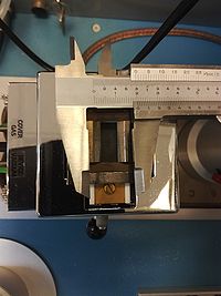
The Cammax EDB80 Die bonder is for placing and soldering dies onto a package or substrate.
The bonder has a graphite heater element enabling fast heating to the melting point of the solder. To prevent oxidation of the solder and bonding surfaces it is possible to have a gas flow of formier gas (4-10% H2 in N2) over the sample. The machine also has a pick-up tool enabling accurate placement of the sample onto a carrier.
The user manuals, user APVs, technical information and contact information can be found in LabManager:
Process information
Flip-chip bonder (glue attachment)
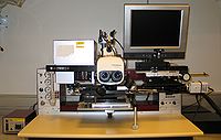
The flip chip bonder can be used to place chips on a substrate with high precision. This way electrical contacts can be made between contact pads on the chip and substrate.
With a dispensing tool small amounts of solder paste or glue is dispensed on the substrate with high accuracy. The substrate could for example be a printed circuit board (PCB). After some experience with the machine, it is possible to place dots with different shapes and sizes on the surface. With a placement tool a chip can then be picked up upside down and by the use of a camera unit, it is possible to align the contacts on the chip to the solder/glue dots on the on the substrate before joining the two surfaces with a light pressure. The stack is subsequently cured and an underfill glue can be dispensed to enhance the bonding strength between chip and substrate.
The Flip Chip Bonder is placed in Danchip's Packlab building 347, 1. floor.
The user manuals, user APVs, technical information and contact information can be found in LabManager:
Flip-chip Bonder in LabManager
| Equipment | Die bonder | Flip-chip bonder | |
|---|---|---|---|
| Purpose |
|
| |
| Performance |
|
| |
| Substrates | Allowed materials |
|
|


