Specific Process Knowledge/Thin film deposition/DiamondCVD/Diamond CVD process details
Feedback to this page: click here
All contents by DTU Nanolab staff unless otherwise noted.
Diamond growth by MPCVD at Nanolab
At Nanolab, it is possible to grow single- and polycrystalline diamond in the SEKI diamond CVD. The diamond CVD applies microwaves to create plasma in a mix of H2, CH4 and O2 gas. This reactive mix allows diamond to grow from an existing diamond lattice.
Diamond formation
Diamond is grown by depositing carbon from the CH4 on a substrate. If the carbon forms an sp3 bond to other carbon atoms, diamond is grown. Otherwise it will be etched away by a high concentration of H2. Diamond is very inert, but the plasma in the CVD equipment creates hydrogen radicals that in turn create active sites on the diamond surface. These active sites react with methane radicals that are also created in the plasma. In practice oxygen is also introduced to the chamber and helps the diamond grow.
In order to obtain diamond bonds the temperature has to be sufficiently high. If the temperature is too low the carbon will fond sp2 bonds and will result in so-called "diamond-like carbon".
Poly- and single crystalline diamond
Polycrystalline diamond
For polycrystalline growth the substrate must be seeded with diamonds. This is commonly done by sonicating the substrate in a solution of water with nano diamonds, although other solvents may give better results (see this paper). After sonication the substrate is rinsed and blow-dried.
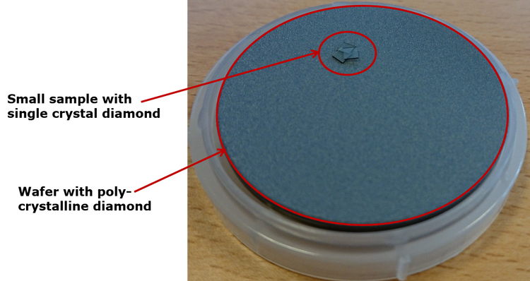
Note that the substrate must be able to withstand high temperature (at least 700°C) and also high temperature gradients, as the center of the substrate is heated more than the edges. In practice this means that to grow diamond on Si it is necessary to use a thick Si substrate (see image of a thick poly-Si sample on the right). Ordinary 500 micron thick 2" wafers break due to stress induced by the temperature gradient.
Polishing is needed after deposition if the polycrystalline diamond layer has to be smooth. This cannot be done here at Nanolab, so the film must be sent away for polishing. Following polishing it is possible to etch the film in the metal ICP, but etching cannot take the place of polishing as different crystal faces of the diamond etch at different rates.
Thinning is needed if the diamond layer has to be very thin because a uniform diamond layer can only be deposited above 1 μm thickness.
Single crystal diamond
It is possible to grow very clean diamond in the SEKI system which should be usable for thermal and perhaps optical applications. To grow single crystal diamond we must use a single crystalline diamond substrate (these are purchased and typical dimensions might be 2x2 mm with 0.1 mm thickness, see photo). We have not investigated whether it is possible to distinguish the transition from the purchased substrate to the newly grown layer.
We cannot grow diamond for quantum applications here at Nanolab as we cannot control the N2 dopant level and dopant depth. This would require that we have our own hydrogen generator or that we buy (very expensive) extra pure bottled hydrogen. To control doping levels it is necessary to use 7N hydrogen and to mix it with a very small additional flow of hydrogen which again is mixed with only a few percent nitrogen. The hydrogen we have for general processing at Nanolab contains too much nitrogen. Nitrogen doping affects the optical and electronic properties of the diamond. For instance this can be used in magnetic sensors, which is a topic of research at DTU Physics.
