Specific Process Knowledge/Thin film deposition/Deposition of Tungsten/Sputtering of W in Sputter Coater 3
Feedback to this page: click here
This page is written by Evgeniy Shkondin @DTU Nanolab if nothing else is stated.
All images and photos on this page belongs to DTU Nanolab.
The fabrication and characterization described below were conducted in 2022 by Evgeniy Shkondin, DTU Nanolab.
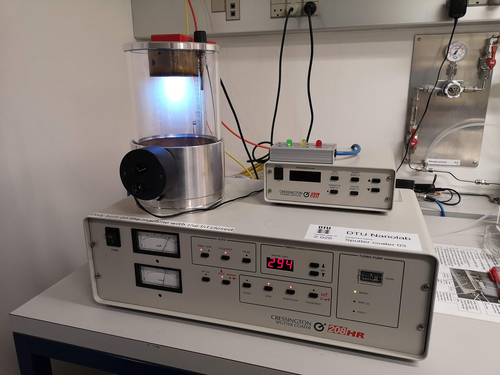
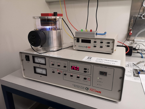
Sputter coater 03 is mainly used for sample preparation before SEM inspection. Usually, Au is sputtered on dielectric surfaces to compensate for charge build-up. Alternatively, many other materials can be sputtered if the setup allows (you need to have a turbo pump and Ar gas). Gold can be deposited even in pure oxygen plasma and only with roughing pumps. Fortunately, Sputter Coater 3 located in the basement of building 346, has both a turbo pump and an Ar working gas source. The pressure during the process is measured to be below 0.1 mBar. This page describes deposition of tungsten (W) with this instrument.
The prepared samples were investigated by the X-ray Reflectivity (XRR), Scanning Electron Microscopy (SEM) and Photo Electron Spectroscopy (XPS) methods. The focus of the study was the deposition conditions.
It is recommended to clean the target with fine sandpaper to remove the native oxide if the target was not used for a long time.
In summary, the tungsten films produced by Sputter-Coater 3 are of poor quality. The user can install a big (15 cm high glass chamber). In this case, the deposition rate is very low (0.033 nm/s) and the film will contain a high level of oxygen (up to 50%). This can be partially improved by installing a smaller chamber (6.5 cm high). However, this leads to a very bad uniformity disregardless of which current settings are used. Depositing on small samples (around 1x1 cm) placed in the middle of the chamber will be the most acceptable procedure. Nevertheless, the elevated level of oxygen and rough and porous structure will limit the applicability.
Tungsten (W) from Sputter Coater 3 is not recommended as a part of sample preparation before SEM inspection. It is better to use Au.
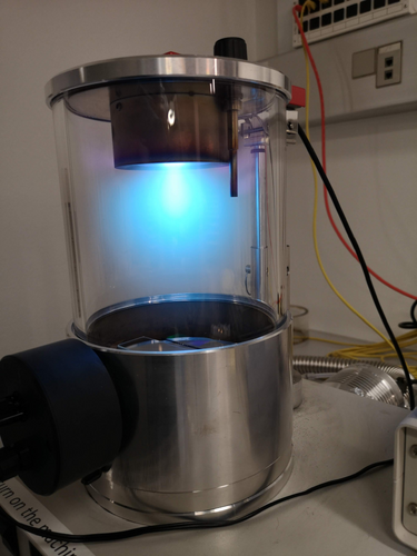
Big glass configuration (15 cm high)
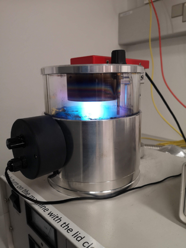
In the beginning, a big glass chamber was installed in the instrument. It was quickly revealed that the deposition rate is very low, so only the highest current setting (80 mA) was used in the experiment.
The maximum time the user can select is 300s, so if longer depositions are needed the user has to redo it several times to achieve an expected thickness.
- Big glass chamber setup.
Big glass configuration.
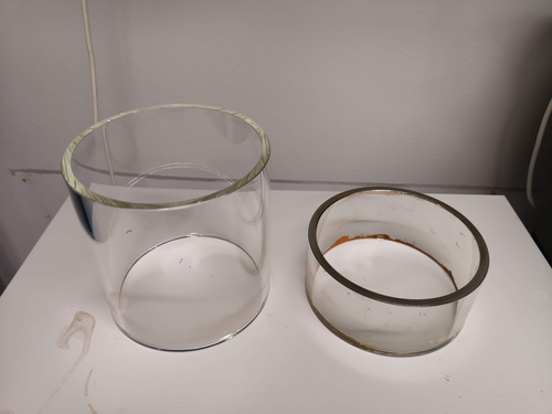
Big (15 cm) and small (6.5 cm) glass chambers.
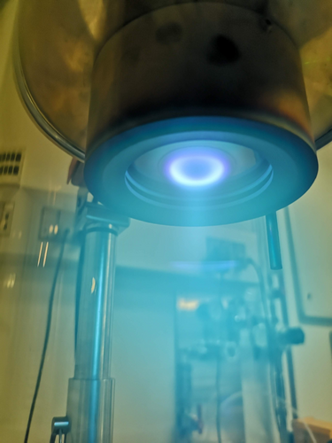
Plasma confinement. Formation of the "race track".
Glow discharge in the deposition chamber.


SEM Inspection
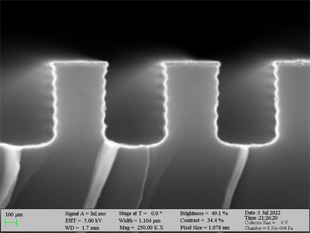
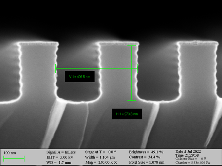
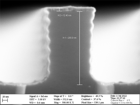
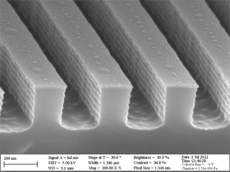
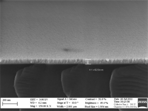
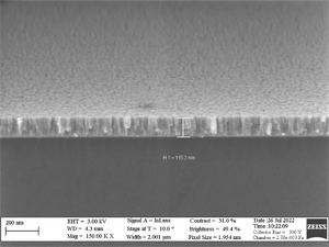
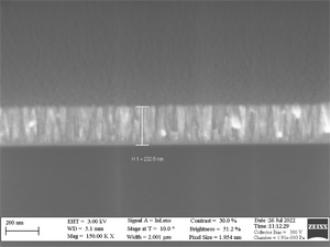
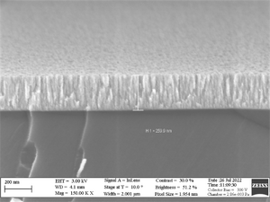
The samples with low aspect ratio Si trenches (500 nm deep, 200 nm wide with a pitch of 400 nm) were used to illustrate the deposition morphology (Instrument: SEM Supra 1). To make the result more visible it was deposited twice at the maximum allowed deposition time (2x300s). The SEM results are shown below.
- Deposition of W on low aspect ratio Si trench structures.
SEM image. 80mA 300s+300s deposition time.
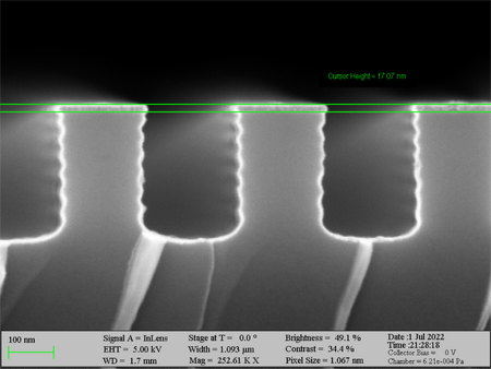
SEM image. 80mA 300s+300s deposition time.
SEM image. 80mA 300s+300s deposition time.
SEM image. 80mA 300s+300s deposition time.
SEM image. 80mA 300s+300s deposition time. Tilted view.
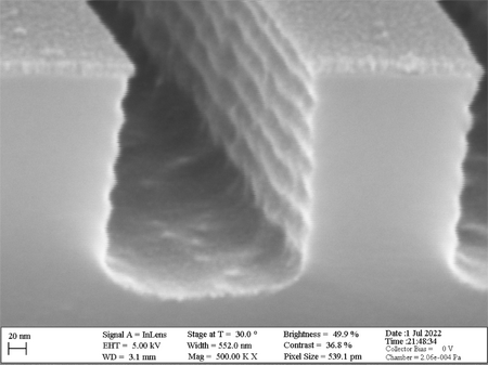
SEM image. 80mA 300s+300s deposition time. Tilted view.


X-ray Photoelectron Spectroscopy
X-ray photoelectron spectroscopy (Instrument: XPS K-Alpha) has been applied to investigate the chemical content and stoichiometry.
The samples used for the XPS analysis were prepared in a big glass chamber with 80mA current and a deposition time of 300s.The pressure is measured to be below 0.1 mBar.
The analysis reveals that the top surface is a native oxide, while the thin layer itself is partially oxidized tungsten. The stoichiometry shows 50%W and 50% O. The stoichiometric tungsten oxide has a form of WO3, so the layer itself contains metallic W around 33% mixed with up to 67% oxide. This is not a big surprise since this tool does not have shutter mechanisms or a long well controlled pumping system. The deposition rate is also very low due to the limited power. This also contributes to the elevated oxygen level in the film.
- XPS depth profile of W thin film. Indicates the presence of native W oxide, the W thin film, and silicon substrate with native oxide.
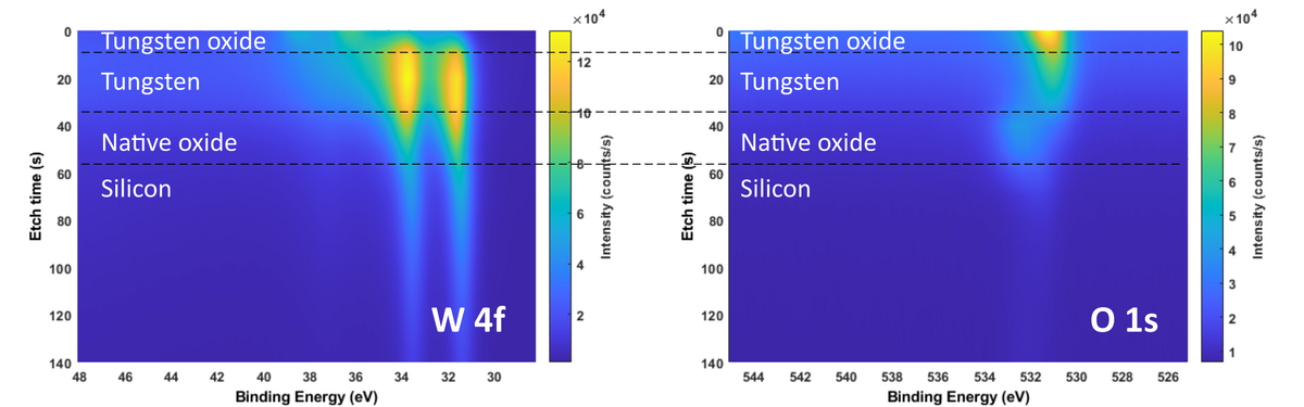
High-resolution scans of W4f and O1s.

- XPS scans.
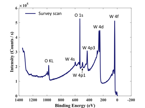
Survey scan.
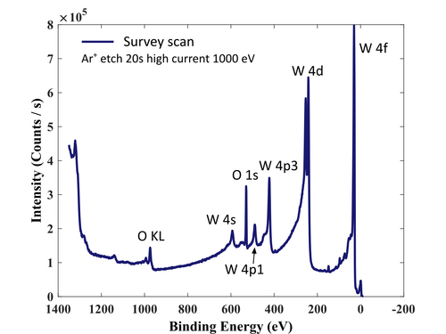
Survey scan after 20s of Ar etch.


X-ray Reflectivity
The samples used for X-ray analysis (Instrument: XRD SmartLab) were prepared in a big glass chamber with 80mA current and a deposition time of 300s.
X-ray reflectivity (XRR) profiles for W films at two different positions on the 100mm wafer have been obtained using the Rigaku XRD SmartLab equipment. The voltage and current settings for the Cu X-ray tube were standard 40kV and 30mA. The incident optics contained a IPS (incident parallel slit) adaptor with 5 ° Soller slit. Other slits: IS=0.03mm RS1=0.03mm and RS2=0.075mm. Step size: 0.01 and measurement time - 5s for each point. Fitting procesure was performed using the commercial GlobalFit software assuming the model based on a Si substrate with native oxide followed by the deposited W film with thin oxides and moisture surfaces. The results are summarized in a table below.
| X-ray analysis result (100mm Si wafer) | ||||||||||||||||||||||||||||||||||||||||||||||||||||||||||||||||||||||||||
| ||||||||||||||||||||||||||||||||||||||||||||||||||||||||||||||||||||||||||

- Big glass chamber. 100mm wafer loaded. X-ray analysis.
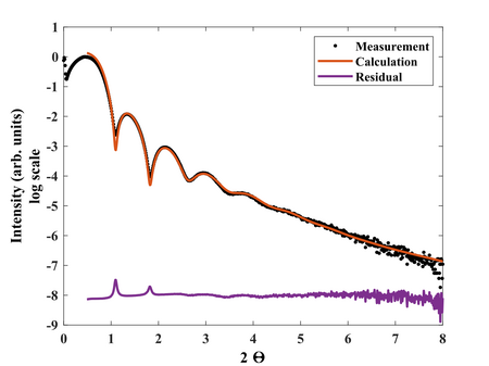
300s, 80mA. Center of the wafer.
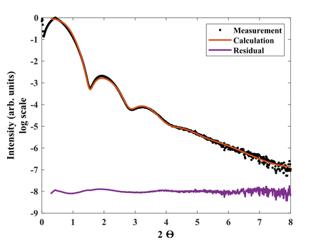
300s, 80mA. Edge of the wafer.
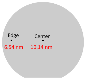
Uniformity of W thickness across a 100 mm wafer in the big glass configuration.


The fitted value of the tungsten density (5-8 g/cm3) is much less than the bulk value of pure W which is 19.25 g/cm3. This low value is very similar to the density of stoichiometric tungsten oxide WO3 which is 7.16 g/cm3. XPS however proves that 67% of the film contains tungsten oxide and 33% W, so this low density can not be explained by the oxidation event only. The most logical explanation is to assume that the layer is not very dense. It contains a lot of nanopores, grain imperfections, etc.
Deposition rate and Uniformity
- Deposition rate of W at 80 mA in a big glass (15 cm high) configuration is 0.033 nm/s. The uniformity variation across a 100 mm wafer is up to 50%. The pressure is measured to be below 0.1 mBar.
Small glass configuration (6.5 cm high)
In the next part of the experiment, a small (6.5 cm high) chamber was installed in the instrument. The deposition rate is much higher in this case, so the different current settings (20-80 mA) were employed. The consequence of the higher deposition rate was a very bad uniformity, such as the center of the wafer getting a full thickness, while the edges of the wafer were not covered at all. This deposition mode is better suited for small samples/chips. The produced films revealed high roughness and pronounced porosity revealed by XRR.
- Small glass chamber setup.
Small glass configuration.
Glow discharge in the deposition chamber.


SEM Inspection
- Small glass chamber setup. Flat films deposited on a Si wafers at different current settings.
20mA, 300s deposition time.
40mA, 300s deposition time.
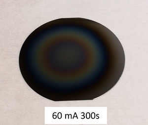
60mA, 300s deposition time.
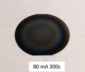
80mA, 300s deposition time.


Deposition rate and Uniformity
- Small glass chamber setup. Flat films deposted on a Si wafers at different current settings.
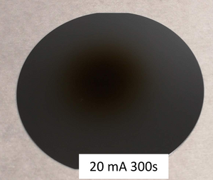
20mA, 300s deposition time.
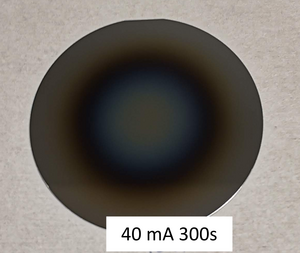
40mA, 300s deposition time.
60mA, 300s deposition time.
80mA, 300s deposition time.


To measure the deposition rate the samples were cleaved, and only the center part was inspected, as the edges almost do not have a layer.
- Small glass chamber setup. Deposition rate as a function of current.
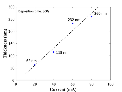
Thickness as a function of current. Measured after 300s deposition, in the middle of the sample.
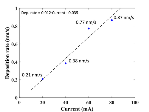
Deposition rate as a function of current. Measured after 300s deposition, in the middle of the sample.


X-ray reflectivity
Deposition of W in Sputter Coater 3 using a small glass (6.5cm high) glass chamber configuration is fast, but the resulting coatings are still expected to have a significant fraction of oxygen. Although XPS measurements were not performed on these films, the sheet resistance values were very high if compared with pure tungsten layers.
- Small glass chamber. 100mm wafer loaded. X-ray analysis.
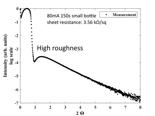
80mA, 150s.

Another issue is the pronounced roughness. The attempt to perform XRR on the film (which is expected to be in the range of 120-130nm) reveals a very clear rough layer profile, where all oscillations were canceled, and a smooth curve of reflected intensity was observed. These findings support the conclusion that produced films are porous and partially oxidized.