Specific Process Knowledge/Thin film deposition/Deposition of Silicon Carbide/Deposition of SiC in Sputter-System Lesker
Feedback to this page: click here
This page is written by Evgeniy Shkondin @DTU Nanolab if nothing else is stated.
All images and photos on this page belongs to DTU Nanolab.
The fabrication and characterization described below were conducted in 2022 by Evgeniy Shkondin and Patama Pholprasit, DTU Nanolab.
We can deposit SiC by RF sputtering in Sputter-System (Lesker). A 2-inch target from gun 5 (RF) is used in the process. Since the material is dielectric we are using 60W power and the slow power ramp. The deposition rate is very slow (0.0056 nm/s), so the oxygen absorption during the process can be an issue.
The prepared samples were investigated by the X-ray Reflectivity (XRR), Spectroscopic Ellipsometry (SE) and X-ray Photo Electron Spectroscopy (XPS) methods. The focus of the study was the deposition conditions.
Recipe:
- Power: 60 W (Maximum allowed)
- Pressure: 3 mTorr
- Power rump: 0.3 W/s
- Deposition mode: RF
- Deposition time: 1800s and 3600s
- Substrate: 4-inch Si and 4-inch Si + 300nm thermal SiO2
In this experiment, two depositions have been made:
- In the first, the 4-inch Si wafer has been used with 1800s deposition time.
- In the second, the 4-inch wafer with 300 nm dry thermal oxide has been used with a 3600s deposition time.
The reason to use a Si wafer with 300nm thermal oxide in the second deposition, was to perform a better fit in ellipsometry. It was difficult to perform the thickness measurement using ellipsometry on the first wafer (1800s deposition). This is why the thicker layer has been deposited on the sample that contained 300nm SiO2. This is a rather known approach to measuring thicknesses on absorbing layers like thin metallic coatings etc. Later, the X-ray Reflectivity (XRR) was performed on both wafers to state the correct thicknesses and structure.
X-ray Reflectivity
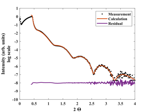
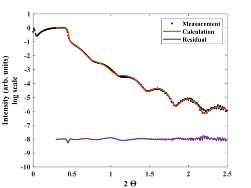
X-ray Reflectivity (XRR) analysis of both samples (the 1800s on Si and 3600s on Si with 300nm SiO2) have been performed to investigate the thicknesses, roughness, and density profiles.
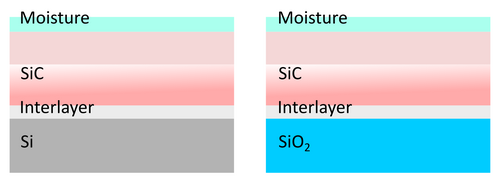
The second wafer that contained Si with 300nm SiO2 was considered to have an infinitly thick glass coating since 300nm thickness is too hard to resolve with our X-ray optics.
The scans has been obtained using Rigaku XRD SmartLab equipment. The voltage and current settings for the Cu X-ray tube were standard 40kV and 30mA. The incident optics contained a IPS (incident parallel slit) adaptor with 5 ° Soller slit. Other slits: IS=0.03mm RS1=0.03mm and RS2=0.075mm. Step size: 0.01 and measurement time - 5s for each point. Fitting procesure was performed using commercial GlobalFit software assuming the model based on Si or SiO2 substrates with native oxide/interlayer followed by the deposited SiC film (with varying density) with thin oxides and moisture surfaces. The results are summarized in a tables below.
| X-ray analysis results of both samples (1800s on Si and 3600s on Si with 300nm SiO2) | ||||||||||||||||||||||||||||||||||||||||||||||||||||||||||||||||||||||||||||||||||||||||||||||||||||||||||||||||||
| ||||||||||||||||||||||||||||||||||||||||||||||||||||||||||||||||||||||||||||||||||||||||||||||||||||||||||||||||||

- Big glass chamber. 100mm wafer loaded. X-ray analysis.
300s, 80mA. Center of the wafer.
300s, 80mA. Edge of the wafer.
Uniformity of W thickness across 100 mm wafer in the big glass configurtion.


It is clear that the SiC film possesses a complicated structure, where density is not constant but instead has a strange gradient. With this assumption, we cloud fit the XRR data nicely.
Deposition rate
Deposition rate for SiC at 60W power (RF) and 3 mTorr presssure is 0.0056 nm/s
Optical functions
Optical functions of deposited SiC were fitted with four Lorentz oscillators. Equipment used: Ellipsometer VASE
- Optical functions of SiC thin film (3600s).
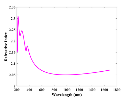
Refractive index.
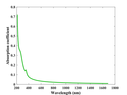
Absorption coefficient.


X-ray Photoelectron Spectroscopy
XPS measurements of both samples has been performed using XPS K-Alpha equipment. The purpose of the investigation is to get an idea about film stoichiometry and possible contamination. Oxygen is present in the film (up to 30 at.%) due to limited deposition rate.
- XPS recordings. 10 nm SiC deposited on Si wafer
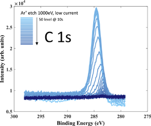
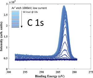
C 1s signal.
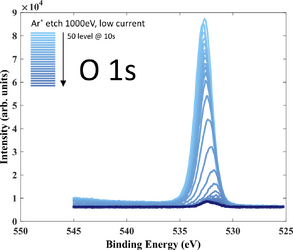
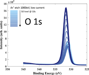
O 1s signal.
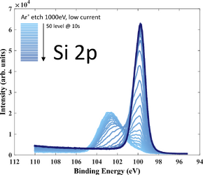
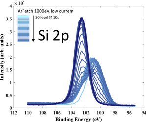
Si 2p signal.
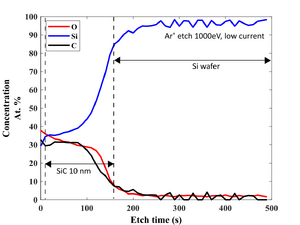
Stoichiometry as a function of depth.


- XPS recordings. 10 nm SiC deposited on Si wafer
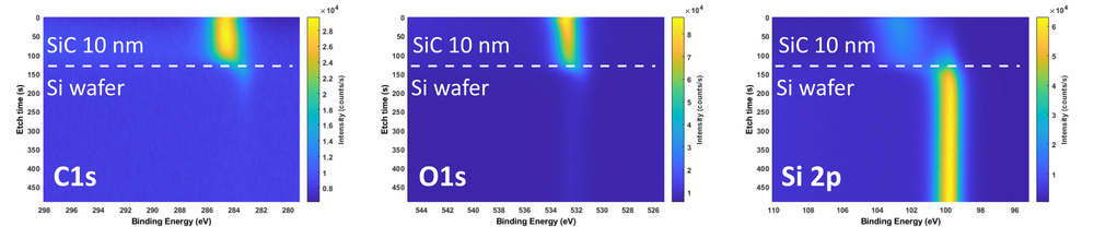
High Resolution signal recording. 2D image.

- XPS recordings. 20 nm SiC deposited on 300 nm thermal SiO2
C 1s signal.
O 1s signal.
Si 2p signal.
Stoichiometry as a function of depth.


- XPS recordings. 20 nm SiC deposited on 300 nm thermal SiO2
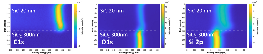
High Resolution signal recording. 2D image.

Process recordings
- Deposition recordings.
Ar flow recording. Thin layer (1800s deposition time).
Pressure recording. Thin layer (1800s deposition time).
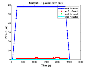
Forward and reverse power recordings. Thin layer (1800s deposition rime).
DC bias recordings. Thin layer (1800s deposition time).
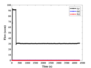
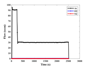
Ar flow recording. Thick layer (3600s deposition time).
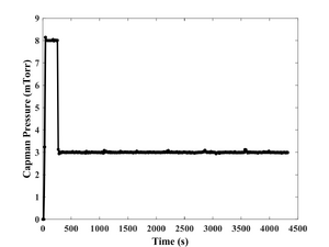
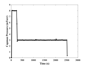
Pressure recording. Thick layer (3600s deposition time).
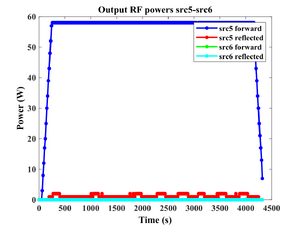
Forward and reverse power recordings. Thick layer (3600s deposition time).
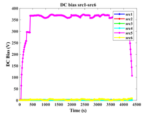
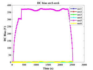
DC bias recordings. Thick layer (3600s deposition time).


