Specific Process Knowledge/Thin film deposition/Deposition of Silicon/Si sputter in Sputter-System Lesker
Feedback to this page: click here
This page is written by Evgeniy Shkondin @DTU Nanolab if nothing else is stated.
All images and photos on this page belongs to DTU Nanolab.
The fabrication and characterization described below were conducted in 2022 by Evgeniy Shkondin, DTU Nanolab.
Sputtering of Si in the Sputter-System (Lesker)
Si can be DC or RF sputtered in the Sputter-System (Lesker) as well as in the Wordentec and the new cluster sputter system. You will find information on the pressure, max power and expected deposition rate for the Sputter-System Lesker here in LabAdviser. To see all the deposition parameters used by others, search the Process Log in LabManager.
Sputtering of Si using RF mode
This page presents the results of Si deposition using RF sputtering in Sputter-System Lesker, now commonly known as "Old Lesker". The deposition target is Si. Source #5 (RF) was used. RF-Si is traditionally used for the fabrication of CrSi hard mask for the CORE dry etch process.
The fabrication and characterization described below were conducted in 2021-2022 by Evgeniy Shkondin, DTU Nanolab. The prepared samples were investigated by the Spectroscopic Ellipsometry. The optical model is based on Tauc Lorentz and two Lorentz oscillators (TL+L+L). The focus of the study was the deposition conditions for possible backup in case of Cluster Lesker failure.
The process recipe in a Sputter-System (Lesker) is following:
- Deposition type: RF
- Power: 90 W.
- Pressure: 3 mTorr
- Gas: Ar
- Deposition time: 1800 and 3600 s.
- Temperature: 20°C (no heating)
- Measured DC bias: 427V
Measured thickness: 23nm and 50nm for 1800s and 3600s respectively (Measured by Spectroscopic Ellipsometry. The substrate used: Si wafer with thermally grown 300nm dry SiO2 in C1 furnace)
- Deposition Rate: 0.0139 nm/s
- Uniformity measurements. Thickness distribution across 6-inch wafer.
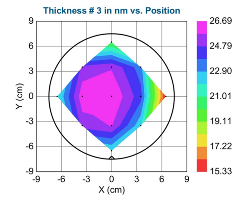
Deposition time 1800s.
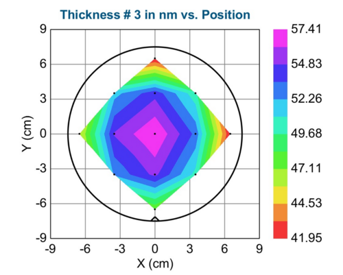
Deposition time 3600s.


- Deposition rate and optical functions for two thicknesses.
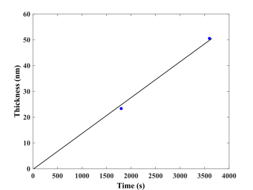
Thickness as a function of time.
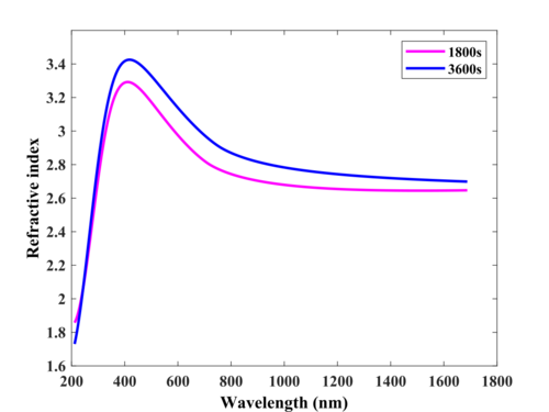
Refractive index.
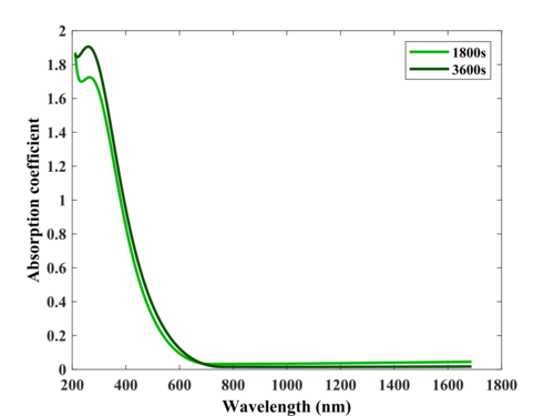
Absorption coefficient.


| Deposition results on 150mm wafers | ||||
|---|---|---|---|---|
| Time (s) | Average thickness (nm) | Standard deviation error | Minimum thickness (nm) | Maximum thickness (nm) |
| 1800 | 23.343 | 3.1715 | 15.326 | 26.687 |
| 3600 | 50.534 | 4.980 | 41.953 | 57.411 |
Surface roughness optimization
By Bjarke Thomas Dalslet @Nanotech.dtu.dk
The Lesker CMS 18 sputter system provides thin films of varying surface roughness. This roughness was verified to be dependent on the sputtered material, sputter mode (DC or RF) and the substrate bias strength. Other probable factors include sputter power and pressure. Below is a table of results for Si. Similar studies were carried out for SiO2 and Ta.
The "From Si target (DC sputter)" study was done on clean Si substrates. The sputter pressure was 3 mTorr using DC reactive sputtering of a Si target. Oxygen was added to the argon sputter gas. Above 10% O2 the gun seems to oxidize at this sputter power. Figure below shows the difference in AFM images between no RF bias (wafer 12) and RF bias (Wafer 21).
From Si target (DC sputter)
| Wafer nr | RF bias (W) | Reactive O2 (%) | Power(W) | Rq (RMS) (nm) | Thickness |
| 12 | 0 | 5 | 135 | 1.44 | 123 nm (ellipsometry) |
| 13 | 0 | 9 | 130 | 1.32 | 98 nm (ellipsometry) |
| 14 | 0 | 13 | 100 | 1.37 | 71.5 nm (ellipsometry) |
| 15 | 10 | 9 | 90 | 0.984 | 56.25 nm (ellipsometry) |
| 21 | 20 | 9 | 90 | 0.112 | |
| 22 | 15 | 9 | 90 | 0.509 |

Stress in Si deposited at high temperature
In 2017, Radu Malureanu investigated stress in a variety of films including Si deposited with the Lesker sputter system. He was able to obtain high tensile stress in Si at 600 °C.
Deposition parameters and results of the study may be found here: *Stress dependence on sputter parameters.