Specific Process Knowledge/Thin film deposition/Deposition of NiV/Sputtering of NiV in Lesker
Feedback to this page: click here
All contents by DTU Nanolab staff. See further attribution below.
NiV is used as a seed layer before Ni electroplating. To initiate the plating process, the surface must be conductive and made of nickel, as it is the plating material. Sputtering is a technique that enables improved step coverage, making it an obvious choice for seed layer preparation. Ni in its pure form will quickly develop a native oxide, which will degrade the plating performance. To avoid oxidation, nickel is replaced by a NiV alloy, where a small amount of vanadium (7 At.%) stabilizes the nickel.
The NiV sputter deposition is highly dependent on the process parameters (Power and Pressure)
by Patama Pholprasit @ dtu nanolab in December 2016
| Power [W] | Pressure [mtorr] | NiV deposition rate [Å/s] | Roughness Ra by AFM [nm] | AFM image | SEM image | Comments |
|---|---|---|---|---|---|---|
| 157 | 5 | 0.833 | 0.546 |  |
 |
|
X-Ray Reflectivity analysis of ultrathin NiV films
by Evgeniy Shkondin @ dtu nanolab in August 2022
In some cases, very thin layers (down to a few nm) of NiV need to be deposited. It is very challenging to measure the thickness since the Dektak profilometer is not sensitive in that range. Alternative methods include AFM or, as in this case, non-destructive X-ray reflectivity measurement (XRR).
This section describes the deposition of a very thin NiV layer, where aimed thickness is 5 nm.
NiV has been sputtered (Source 2 DC) from gun 2 (HSM) in Sputter System (Lesker) with the following parameters: 157W, 3mTorr, and the 60s deposition time. The measured DC bias was 375V
X-ray reflectivity (XRR) profiles for NiV films at two different positions (center and edge) on a 150 mm wafer have been obtained using Rigaku XRD SmartLab equipment. The voltage and current settings for the Cu X-ray tube were standard: 40 kV and 30 mA. The incident optics contained an IPS (incident parallel slit) adapter with a 5° Soller slit. Other slits: IS=0.03mm, RS1=0.03mm, and RS2=0.075mm. Step size: 0.01 and measurement time - 5s for each point. The fitting procedure was performed using commercial GlobalFit software, assuming the model is based on a Si substrate with native oxide, followed by the deposited NiV film with thin oxides and moisture surfaces. NiV density is assumed to be linearly dependent as a function of depth. The results are summarized in the table below.
- Sample model used in XRR analysis.
-
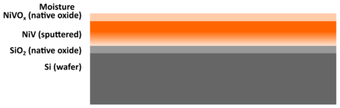 Sample is considered to have NiV layer with oxide top/moisture deposited on natively oxidized silicon.

| Layer parameter list (center point) | |||||||
|---|---|---|---|---|---|---|---|
| Layer name | Thickness (nm) | Density (g/cm3) | Depth distribution | Bottom Density (g/cm3) | Rougness (nm) | Delta | Beta |
| NiVOx (top layer/moisture) | 1.64 |
2.22 | No distribution | 0.35 | 7.2251e-6 | 1.6778e-7 | |
| NiV (sputtered) | 5.95 |
9.00 | Linear | 7.13 | 1.16 | 2.4961e-5 | 5.0462e-7 |
| SiO2 (native oxide) | 0.98 | 1.88 | No distribution | 0.33 | 6.0936e-6 | 7.9412e-8 | |
| Si (wafer) | 2.328 | No distribution | 0.00 | 7.5626e-6 | 1.7561e-7 | ||
| Layer parameter list (edge point) | |||||||
|---|---|---|---|---|---|---|---|
| Layer name | Thickness (nm) | Density (g/cm3) | Depth distribution | Bottom Density (g/cm3) | Rougness (nm) | Delta | Beta |
| NiVOx (top layer/moisture) | 1.65 |
2.28 | No distribution | 0.37 | 7.4468e-6 | 1.7293e-7 | |
| NiV (sputtered) | 5.00 |
8.20 | Linear | 6.41 | 0.97 | 2.2744e-5 | 4.5979e-7 |
| SiO2 (native oxide) | 0.98 | 1.87 | No distribution | 0.33 | 6.0936e-6 | 7.9411e-8 | |
| Si (wafer) | 2.328 | No distribution | 0.00 | 7.5626e-6 | 1.7561e-7 | ||
- XRR analysis of thin NiV.
-
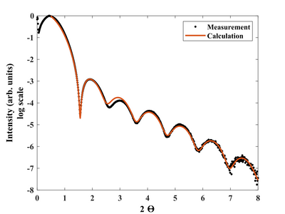 X-ray reflectivity. Measurement and Fit. Center point.
 -
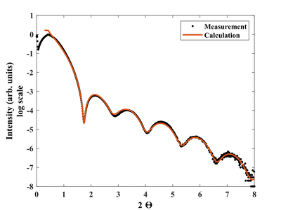 X-ray reflectivity. Measurement and Fit. Edge point.

