Specific Process Knowledge/Thin film deposition/Deposition of Chromium/Sputtering of Cr in Sputter System (Lesker)
Feedback to this page: click here
This page is written by Evgeniy Shkondin @DTU Nanolab if nothing else is stated.
All images and photos on this page belongs to DTU Nanolab.
The fabrication and characterization described below were conducted in 2021-2022 by Evgeniy Shkondin.
Cr Sputtering
This page presents the results of Cr deposition using DC sputtering in Sputter-System Lesker, now commonly known as "Old Lesker". The deposition target is Cr. Source #2 (DC) was used.
The fabrication and characterization described below were conducted in 2021 by Evgeniy Shkondin, DTU Nanolab. The prepared samples were investigated by the X-ray Reflectivity method. The focus of the study was the deposition conditions.
The process recipe in a Sputter-System (Lesker) is following:
- Deposition type: DC
- Power: 220 W.
- Pressure: 3 mTorr
- Gas: Ar
- Deposition time: 360
- Temperature: 20°C (no heating)
- Measured DC bias: 360V
- Deposition Rate: 0.148 nm/s
XRR-measurement
| Layer parameter list | |||||
|---|---|---|---|---|---|
| Layer name | Thickness (nm) | Density (g/cm3) | Rougness (nm) | Delta | Beta |
| Moisture | 1.73 | 0.99 | 0.00 | 3.0119e-6 | 6.9942e-8 |
| Cr2O3 | 4.36 | 2.96 | 0.00 | 8.9602e-6 | 6.2352e-7 |
| Cr | 48.99 |
6.19 | 2.93 | 1.8194e-5 | 1.8712e-6 |
| SiO2 (native oxide) | 2.34 | 3.02 | 1.92 | 9.8053e-6 | 1.2778e-7 |
| Si (wafer) | 2.328 | 0.00 | 7.5795e-6 | 1.7601e-7 | |

- XRR analysis of Cr thin film.
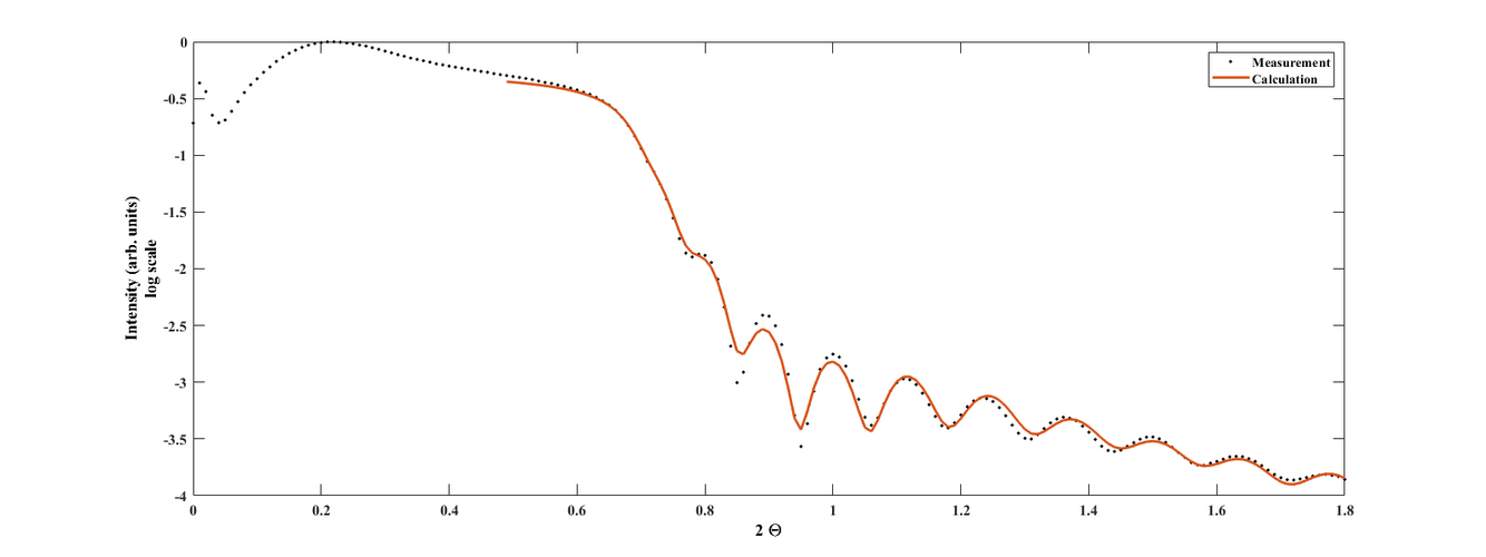
X-ray reflectivity. Measurement and Fit.
