Specific Process Knowledge/Thin film deposition/Deposition of Chromium/Deposition of Chromium
Feedback to this page: click here
Roughness of Cr layers
The result here from Katharina Nilson @ nanolab (August 2008)
Cr have been deposited with both E-beam evaporation and sputtering deposition to examine if there are differences in the roughness of the Cr layers.
Experimental
Cr depositions have been done directly on unprocessed Si wafers, all depositions has been done in Wordentec. The deposited layers have thereafter been examined with AFM.
Results
There are differences in film roughness for the various deposition methods. For the sputtering processes there are large differences depending on the settings during the process, i. e. Ar pressure and effect.
E-beam process
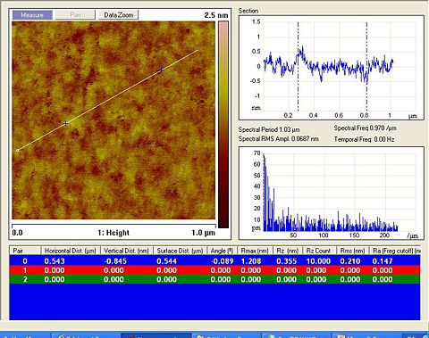
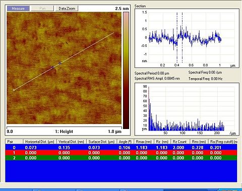
The Cr layer deposited with e-beam in the Wordentec has a low roughness. The deposition rate has been 10 Å/s.

Sputtering process
In the Wordentec the Ar pressure can be set to between and mbar during the process, and the effect may be varied between 150 and 400 W. ( Here are AFM pictures of sputtered layers, deposited with different settings, shown.
Power 150 W, pressure mbar
With these settings the deposited layers are uniform and has a low roughness.

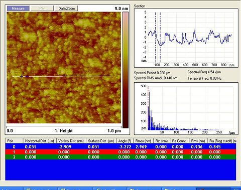
Power 405 W, pressure mbar
405 W and mbar Ar pressure results in a surface with large roughness. The surface grains are comparably small (most about 30 nm in diameter, and almost all below 50 nm).

Power 405 W, pressure mbar
These settings give a rough surface, with larger grains (up to 100 nm in diameter).

Conclusions
The roughness of Cr layers is very different for the sputter depositions with different setting. The layer with lowest roughness is archived by using 150 W and mbar argon pressure. A layer with similar roughness is also the result of an e-beam process (Wordentec). However, the use of sputtering deposition will give a better step coverage than the e-beam process.


