Specific Process Knowledge/Thin film deposition/ALD Picosun R200/AZO deposition using ALD
Feedback to this page: click here
Obsolete - AZO should now be deposited in ALD2
Results on this page can only be used as inspiration. A lot of the hardware has changed a lot since 2016-2017. The DEZ precursor is no longer stored outside the tool cabinet, and instead, we exchange TiCl4 and DEZ, which will unavoidably affect the result. The changes though are supposed to be minor.
From 2022, we prefer that all work involving DEZ is happening in ALD2 instead.
AZO can be deposited in a temperature window 150 - 250 oC. Physical and optical properties are strongly corelated with deposition temperture and Al doping concentration. Research results based on this page information can be found here: LINK Optical Materials Express 7(5), pp. 1606-1627 (2017)
All results shown on this page have been obtained using the Si(100) wafers with native oxide as substrates:
Al-doped ZnO (AZO) deposition overview
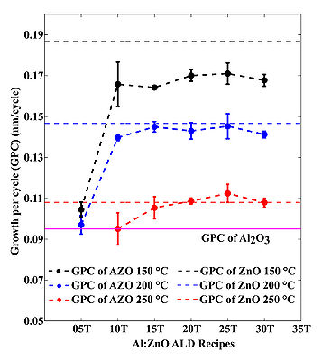
The deposition rate for AZO depends on the temperature and doping concentration, see figures that illustrate AZO growth below. The uniformity, thickness, refractive index has been obtained using Ellipsometer VASE.
-
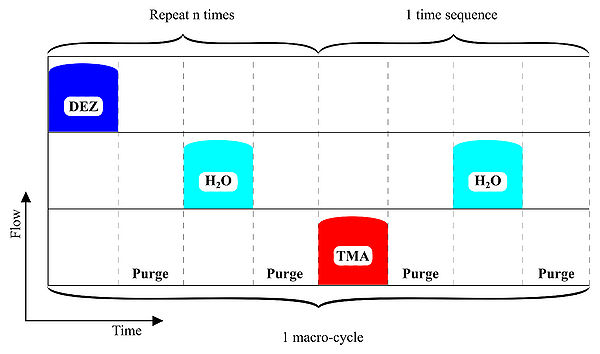 Figure 1. ALD-schematics for AZO deposition.
 -
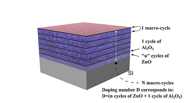 Figure 2. Schematic drawing of deposited AZO layers and concept illustration of doping "D" number/level 05, 10, 15, 20,etc.
 -


Evgeniy Shkondin, DTU Nanolab (former DTU Danchip), 2015-2016.
Al-doped ZnO (AZO) standard recipes
Recipe: AZO 20T
(Number 20 means doping level "D": 19 cycles of ZnO + 1 cycle Al2O3, see details in the table below)
Maximum deposition thickness: 100 nm
Temperature: 150 oC - 250 oC
| # macrocycles | N | |||||||
|---|---|---|---|---|---|---|---|---|
| # cycles | 19 | 1 | ||||||
| Precursor | DEZ | DEZ | H2O | H2O | TMA | TMA | H2O | H2O |
| Nitrogen flow | 150 sccm | 150 sccm | 200 sccm | 200 sccm | 150 sccm | 150 sccm | 200 sccm | 200 sccm |
| Pulse time | 0.1 s | 0.1 s | 0.1 s | 0.1 s | 0.1 s | 0.1 s | 0.1 s | 0.1 s |
| Purge time | 0.5 s | 20.0 s | 0.5 s | 20.0 s | 0.5 s | 20.0 s | 0.5 s | 20.0 s |
How to fill out the process log in LabManager:
The pulse time for each precursor equals the total pulse time times the number of cycles in each macrocycle.
DEZ pulse time: (0.1 + 0.1) s * 19 = 3.8 s
TMA pulse time: (0.1 + 0.1 )s * 1 = 0.2 s
H2O pulse time: [(0.1 + 0.1) s * 19] + [(0.1 + 0.1) s * 1] = 4.0 s
The number of cycles for each precursor now equals the number of macrocycles (n).
Recipe: AZO 25T
Number 25 means doping level "D": 14 cycles of ZnO + 1 cycle Al2O3, see details in the table below)
Maximum deposition thickness: 100 nm
Temperature: 150 oC - 250 oC
| # macrocycles | N | |||||||
|---|---|---|---|---|---|---|---|---|
| # cycles | 24 | 1 | ||||||
| Precursor | DEZ | DEZ | H2O | H2O | TMA | TMA | H2O | H2O |
| Nitrogen flow | 150 sccm | 150 sccm | 200 sccm | 200 sccm | 150 sccm | 150 sccm | 200 sccm | 200 sccm |
| Pulse time | 0.1 s | 0.1 s | 0.1 s | 0.1 s | 0.1 s | 0.1 s | 0.1 s | 0.1 s |
| Purge time | 0.5 s | 20.0 s | 0.5 s | 20.0 s | 0.5 s | 20.0 s | 0.5 s | 20.0 s |
How to fill out the process log in LabManager:
The pulse time for each precursor equals the total pulse time times the number of cycles in each macrocycle.
DEZ pulse time: (0.1 + 0.1) s * 24 = 4.8 s
TMA pulse time: (0.1 + 0.1 )s * 1 = 0.2 s
H2O pulse time: [(0.1 + 0.1) s * 24] + [(0.1 + 0.1) s * 1] = 5.0 s
The number of cycles for each precursor now equals the number of macrocycles (n).
Recipe: AZO 30T
(Number 30 means doping level "D": 29 cycles of ZnO + 1 cycle Al2O3, see details in the table below)
Maximum deposition thickness: 100 nm
Temperature: 150 oC - 250 oC
| # macrocycles | N | |||||||
|---|---|---|---|---|---|---|---|---|
| # cycles | 29 | 1 | ||||||
| Precursor | DEZ | DEZ | H2O | H2O | TMA | TMA | H2O | H2O |
| Nitrogen flow | 150 sccm | 150 sccm | 200 sccm | 200 sccm | 150 sccm | 150 sccm | 200 sccm | 200 sccm |
| Pulse time | 0.1 s | 0.1 s | 0.1 s | 0.1 s | 0.1 s | 0.1 s | 0.1 s | 0.1 s |
| Purge time | 0.5 s | 20.0 s | 0.5 s | 20.0 s | 0.5 s | 20.0 s | 0.5 s | 20.0 s |
How to fill out the process log in LabManager:
The pulse time for each precursor equals the total pulse time times the number of cycles in each macrocycle.
DEZ pulse time: (0.1 + 0.1) s * 29 = 5.8 s
TMA pulse time: (0.1 + 0.1 )s * 1 = 0.2 s
H2O pulse time: [(0.1 + 0.1) s * 29] + [(0.1 + 0.1) s * 1] = 6.0 s
The number of cycles for each precursor now equals the number of macrocycles (n).
Recipe: AZO 35T
(Number 35 means doping level "D": 34 cycles of ZnO + 1 cycle Al2O3, see details in the table below)
Maximum deposition thickness: 100 nm
Temperature: 150 oC - 250 oC
| # macrocycles | N | |||||||
|---|---|---|---|---|---|---|---|---|
| # cycles | 34 | 1 | ||||||
| Precursor | DEZ | DEZ | H2O | H2O | TMA | TMA | H2O | H2O |
| Nitrogen flow | 150 sccm | 150 sccm | 200 sccm | 200 sccm | 150 sccm | 150 sccm | 200 sccm | 200 sccm |
| Pulse time | 0.1 s | 0.1 s | 0.1 s | 0.1 s | 0.1 s | 0.1 s | 0.1 s | 0.1 s |
| Purge time | 0.5 s | 20.0 s | 0.5 s | 20.0 s | 0.5 s | 20.0 s | 0.5 s | 20.0 s |
How to fill out the process log in LabManager:
The pulse time for each precursor equals the total pulse time times the number of cycles in each macrocycle.
DEZ pulse time: (0.1 + 0.1) s * 34 = 6.8 s
TMA pulse time: (0.1 + 0.1 )s * 1 = 0.2 s
H2O pulse time: [(0.1 + 0.1) s * 34] + [(0.1 + 0.1) s * 1] = 7.0 s
The number of cycles for each precursor now equals the number of macrocycles (n).
XPS investigation of AZO thin films
XPS profiles for AZO has been obtained using XPS K-Alpha equipment.
- XPS Investigation of AZO layers.
-
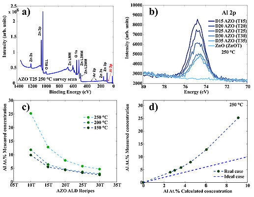 Figure 4. Typical survey scan of AZO/ZnO. b) High resolution scan of the Al 2p region for AZO/ZnO samples prepared at 250 oC c) Measured Al cocncentration in AZO films prepared at three temperatures: 150 oC, 200 oC and 250 oC. d) Deviation of the measured Al at.% concentaration from the theoretical estimation in case of 250 oC deposition temperature. Theoretical estimation can be calculated using following formula: , where GPCAl2O3 and GPCZnO are growth-per-cycle of Al2O3 and ZnO at given deposition temperature, respectively. "D" is a doping level: 05, 10, 15, 20 etc. which corresponds to recipes ...AZO 20T, AZO 25T, AZO 30T.. etc.
 -
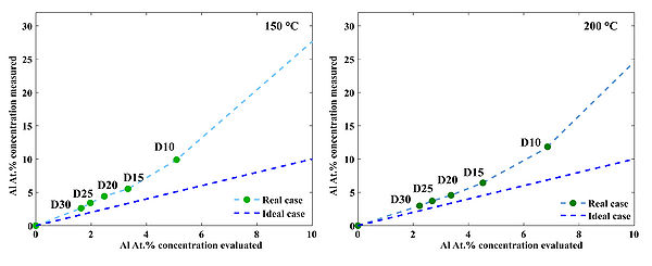 Figure 5. Deviation of the measured Al at.% concentaration from the theoretical estimation in case of 150 oC and 200 oC deposition temperature. Deviations occure due to nucleation issues of ZnO on top of TMA-H2O passiveted surfaces.


| Recipes | 150 oC. Al at.% Concentration mesured using (XPS) | 200 oC. Al at.% Concentration mesured using (XPS) | 250 oC. Al at.% Concentration mesured using (XPS) |
|---|---|---|---|
| ZnOT (no doping) | 0 | 0 | 0 |
| AZO 05T | 30.45 | not measured | not measured |
| AZO 10T | 9.89 | 11.84 | 25.23 |
| AZO 15T | 5.52 | 6.16 | 12.82 |
| AZO 20T | 4.41 | 4.35 | 7.93 |
| AZO 25T | 3.41 | 3.61 | 5.82 |
| AZO 30T | 2.62 | 3.18 | 4.73 |
| AZO 35T | not measured | not measured | 3.98 |
Evgeniy Shkondin, DTU Nanolab (former DTU Danchip), 2015-2016.
Morphology of deposited AZO layers
The surface morphology of deposited 100 nm ZnO/AZO thin films has been analyzed by scanning electron microscopy and atomic force microscopy.
SEM morphology

AFM morphology

AFM inspections of deposited ZnO/AZO films D10-D35 at 250 oC reveals a surface roughness of approx. 2 nm RMS, which slightly decreases with increasing Al content in the films. In case of D10, the Al2O3 phase dominates and it result in a roughness below the acceptable detection value. The AZO films deposited at 250 oC tend to obtain a cylindrical morphology, which can be related to preferred (002) ZnO crystal orientation growth.
Evgeniy Shkondin, DTU Nanolab (former DTU Danchip), 2015-2016.
X-ray diffraction measurements

The crystal orientations have been studied by analyzing X-ray diffraction (XRD) patters. The equipment is D8 diffractometer from Bruker located at DTU Mechanical Engineering Department. θ -2θ scans were acquired in a Bragg-Brentano geometry with a Cu Kα X-ray source. The instrumental broadening was taken into account by performing a LaB6 powder standard scan. The obtained scans were additionally checked for the alignment by controlling the corresponding position of the Si(400) Kα1 and Kβ peaks coming from the Si substrates.
XRD results are summarized in the figure below. It is revealed that AZO films deposited at 250 oC are polycrystalline films with preferential (002) orientation. Two main peaks have been found: (002) and weak (101), all other orientations were not observed in the range 2θ between 20 and 72o. Figure 8(e) below shows, ZnO/AZO XRD obtained patterns at 250 oC.
A (100) peak is observed in the 150 oC deposited films, where this orientation is preferential. In 150 oC AZO films both (100) and (002) peaks are present. XRD results obtained at 150 oC and 200 oC are shown in Figure 8(a) and 8(c). Finally, the (100) orientation vanished at 250 oC and is not observed in Figure 8(e). The noisy part from quasi-forbidden Si (200) reflections has been removed from the scans.
The central positions of the orientation peaks move to higher 2θ values with increasing of Al concentrations in the films. When the concentration becomes too high (like in the case of D15 and D10 recipes processed at 250 oC), the films become amorphous (see Figure 8(a)). Characterization of the crystal structure is conducted by fitting the Lorentzian functions through the (002) and (101) peaks ( see Figure 9(a)). According to the Bragg law:
The d-spacing of a ZnO Wurtzite crystal structure is related to the lattice parameters a and c by:
Here, d is the interplanar distance, h, k and l are Miller indices. The lattice constants of hexagonal Wurtzite unit cell are given by a and c. In this case the (002) and (101) peaks were used to calculate lattice parameters. Figure 8 b), d) and f) show that the a parameter does not undergo any significant changes, while the constant c reduces from 5.20 Å (undoped ZnO) to 5.12 Å (D20) in an almost linear trend. The compression of the lattice constant c is due to the replacement of larger Zn2+ ions by smaller Al3+ ions (ionic radii 72 and 53 pm respectively). The Lorentzian fit through the measured peaks allows the estimation of corresponding grain sizes. The method mostly used is based on the Scherrer equation using either FWHM or integral breadth (area below the peak normalized by its height):
, where:
Here, K is the Scherrer factor, λ is the wavelength of Cu Kα1 radiation, θ is a Bragg angle and βINT is the instrument corrected integral breadth, where βobservedINT and βinstrumentalINT are the corresponding integral breadth of an observed peak and instrumental correction, respectively.

Estimated grain sizes are presented in Figure 9 (b) for all investigated temperatures. Grains with (002) orientations are 2-3 times smaller than corresponding (100) oriented grains. It seems that for AZO films the (002) grains becomes larger with increasing Al concentration, until 4 at.% of Al, then the grain size decreases. (101) oriented crystallites sizes were not calculated due to bigger uncertainties.

Evgeniy Shkondin, DTU Nanolab (former DTU Danchip), 2015-2016.
Electrical properties
A Conventional four-point probe was used for resistivity measurements. A strong correlation between resistivity, Al concentration, and grain size has been found (see Figure10). Undoped ZnO 100 nm films have a resistivity of 8 mOhm.cm, except ZnO grown at 250 oC . The high resistivity of this particular film is believed to be caused by an existence of small pores in the film. The existence of small pores around bigger ZnO clusters is visible in the SEM image in Figure 6.
For 100 nm thick AZO films the lowest resistivity of 1.3-1.4 mOhm.cm is achieved at the Al doing level around 4 at.%. In general, the resistance of 150oC prepared films are higher compared to 200 oC and 250 oC prepared films (Figure 10 a).
Figure 10 b) shows the dependencies between (002) and (100) grains sizes and resistivity. The general trend is that the larger the grains the lower the resistivity, which is observed for both orientations, regardless of growth temperature. The larger the grains, the lower the resistivity.

Evgeniy Shkondin, DTU Nanolab (former DTU Danchip), 2015-2016.
Optical properties
The optical characterization of AZO films has been done using spectroscopic ellipsometry. Figure 11 illustrates the results for 100 nm AZO films grown at 250 oC (results for 200 oC and 150 oC presented in Figures 12 and 13, respectively.
Figure 11 a) illustrates the real and imaginary part of the permittivity for ZnO and AZO films. It shows that the permittivity of AZO decreases rapidly with increasing wavelength, while the permittivity of ZnO remains rather stable.
Figure 11 b) displays the transmission spectra for 100 nm AZO films grown at 250 oC on fused silica (quartz). In this experiment, the ellipsometer was used in transmission mode, where the moving arms of the source and detector were placed at 90o to the surface normal. In the visible wavelength range, all of the films exhibit an average optical transmittance greater than 90%. The spectrum shows a sharp absorption edge in the ultraviolet range, which shifts to the shorter wavelengths (blue shift), as the concentration of Al in the AZO samples increases. The absorption edge can be used to estimate an optical bandgap of AZO thin films. Since ZnO is a direct bandgap semiconductor material, it can reasonably be assumed that the absorption coefficient and the Tauc relationship are given by:
These relations are plotted in Figure 11 c) and d). The energy bandgap can be obtained by plotting vs. and linearly extrapolating the fit of the linear region to as shown in Figure 11 d. As it displayed in Figure 11 e), the higher the Al concentration in the film, the higher the optical bandgap. It can be explained by the increase of the carrier concentration which is caused by Al-doping. This widening of the optical bandgaps is generally attributed to the Burstein-Moss shift effect.


Evgeniy Shkondin, DTU Nanolab (former DTU Danchip), 2015-2016.