Specific Process Knowledge/Etch/Etching of Silicon Oxide/SiO2 etch using AOE/Standard recipe with resist mask/Images of m resist etches
< Specific Process Knowledge | Etch | Etching of Silicon Oxide | SiO2 etch using AOE | Standard recipe with resist mask
Jump to navigation
Jump to search
Feedback to this page: click here
Here are presented some images of etches using the recipe SiO2_res
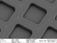
Profile of 1-10µm deep etch + resist profile
by Berit Herstrøm (BGHE) from nanolab
- Old AZ5214E resist (negative - I think), etched for 10 min with SiO2_res at 0 dg. with spacers 30 mm

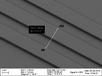
- January 2018 by BGHE, SiO2_res@0degrees, etch time: 4 min, 0mm spacers
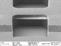


Resist mask effected by m_res_ny
by bghe@nanolab
 Process date: May 2011 Recipe: m_res_ny@0degrees Process time: 30 min Mask: AZ resist 4 µm. Explanation: the surface of the resist gets UV hardened by the plasma. Later the resist gets hot and starts floating - some liquid evaporates. When the wafer cools again the resist shrinks but the hardend surface cannot shrink so it contracts instread giving rise to these creases/folds. |
|---|
Resist mask baked at 150dg effected by m_res_ny
by bghe@nanolab
 Process date: July 2011 Recipe: m_res_ny@0degrees Process time: 30 min Mask: AZ resist 4 µm thick The wafer was preheated to 150dg for 5min. Explanation:The pretreatning makes the resist float and liquid evaporates. Then during the plasma processing there is no more liquid that evaporates and the surface do not contract during cool off. This gives more smooth edges between the wafer and the resist but the profile is more round giving more angled profiles of the oxide etch. |
 Process date: July 2011 Recipe: m_res_ny@0degrees Process time: 30 min Mask: AZ resist 4 µm thick The wafer wafer preheated to 150dg for 5min. Explanation:The pretreatning makes the resist float and liquid evaporates. Then during the plasma processing there is no more liquid that evaporates and the surface do not contract during cool off. This gives more smooth edges between the wafer and the resist but the profile is more round giving more angled profiles of the oxide etch. |
|---|
Etching of 1.0 µm SiO2 by 15 min m_res_ny: Artefacts from Lithography
by Frederik Stöhr @danchip
General Description
- Process date: Jan 2015
- Recipe: m_res_ny@0degrees
- Process time: 15 min
- Substrate: 525 µm Si + 1 µm thermal silicon oxide + ~50 nm BARC (anti reflection coating, which promotes adhesion)
- Mask: [XOP12] AZ5214E positive resist 1.5 µm thick (6-inch aligner 3 sec exposure, 60 sec developer)
- Etch Load (Total Exposed SiO2): ~ 10 %
- Post process: O2 Plasma Ashing 10 min
 The view tilt angle is 40 degrees. According to the original mask design the dots should not be hollow. Nevertheless, during lithography interference effects must have caused the center of the dots to be exposed. Obviously, this artefact is so pronounced that it is also transferred in the subsequent structuring of the silicon oxide. |
|---|


Etching of 1.1 µm SiO2 by 10 min m_res_ny: Corrugated sidewall
by Frederik Stöhr @danchip
General Description
- Process date: Feb 2014
- Recipe: m_res_ny@0degrees
- Process time: 5:30 min
- Substrate: 525 µm Si + 1.1 µm thermal silicon oxide + HMDS (adhesion promoter)
- Mask: [XOP3] AZ positive resist 1.5 µm thick (6-inch aligner 3 sec exposure, 60 sec developer)
- Etch Load (Total Exposed SiO2): ~ 10 %
- Post process: O2 Plasma Ashing 10 min
 Close up. Bird View. Dark area is Silicon. Bright area is Silicon Dioxide. Residues of the SiO2 etching are apperent on top of the SiO2, i.e. particles a few nanometers in diameter. Most probably it is sputtered and redopsited Silicon Dioxide, but not confirmed. Attempts to remove them in 7-Up or HCl failed. |
|---|


Etching of 2.1 µm SiO2 by 10 min m_res_ny: PR mask shape
by Frederik Stöhr @danchip
General Description
- Process date: Feb 2013
- Recipe: m_res_ny@0degrees
- Process time: 10 min
- Mask: [XOP2] AZ5214E positive resist 2.2 µm thick (6-inch aligner 4 sec exposure, 70 sec developer)
- Etch Load (Total Exposed SiO2): ~ 10 %
- Post process: None


Etching of 2.1 µm SiO2 by 12 min m_res_ny: Etch residues
by Frederik Stöhr @danchip
General Description
- Process date: April 2014
- Recipe: m_res_ny@0degrees
- Process time: 12 min
- Substrate: [XOP5] 525 µm Si + 2 µm thermal silicon oxide + HMDS (adhesion promoter)
- Mask: AZ5214E positive resist 2.2 µm thick (6-inch aligner 4 sec exposure, 70 sec developer)
- Etch Load (Total Exposed SiO2): ~ 10 %
- Post process: O2 Plasma Ashing 10 min


Etching of 2.8 µm SiO2 by m_res_ny with AZ5214E mask
by Frederik Stöhr @danchip
General Description
- Process date: May 2014
- Recipe: m_res_ny@0degrees
- Process time: 16 VS 20 min
- Substrate: 525 µm Si + 2.8 µm thermal silicon oxide + HMDS (adhesion promoter)
- Mask: AZ5214E positive resist 2.2 µm thick (6-inch aligner 4 sec exposure, 70 sec developer)
- Etch Load (Total Exposed SiO2): ~ 10 %
- Post process: O2 Plasma Ashing 10 min


Etching of 2.8 µm SiO2 by m_res_ny with AZ MiR 701 mask
by Frederik Stöhr @danchip
General Description
- Process date: May 2014
- Recipe: m_res_ny@0degrees
- Process time: 15:30 min
- Substrate: 525 µm Si + 2.8 µm thermal silicon oxide + HMDS (adhesion promoter)
- Mask: [XOP6] MiR 701 positive resist 2.0 µm thick (KS aligner 29 sec exposure, TMAH Manual MiR701 60s)
- Etch Load (Total Exposed SiO2): ~ 10 %
- Post process: O2 Plasma Ashing 10 min


Etching of 2.2 µm SiO2 by SIO2_RES 10 min VS 15 min
by Frederik Stöhr @danchip
General Description
- Process date: Jan 2015
- Recipe: SIO2_RES@0degrees
- Process time: 10 min VS 15 min
- Substrate: 525 µm Si + 2.2 µm thermal silicon oxide + HMDS (adhesion promoter)
- Mask: [XOP8] AZ5214E positive resist 2.2 µm thick (6-inch aligner 4sec exposure, 60s developer)
- Etch Load (Total Exposed SiO2): ~ 10 %
- Post process: None


