Feedback to this page: click here
This page is written by Berit Herstrøm @ DTU Nanolab (BGHE) if nothing else is stated
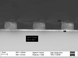
 Process date: February 2012 Recipe: m_poly@60degrees Process time: 25 min Mask: Poly Si 1.8 µm Etch depth: 12.5 µm Line width mask: 25µm Line with after etch: 21.8µm |
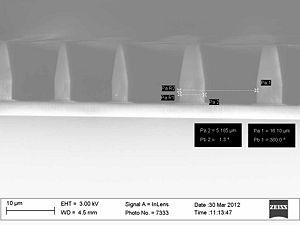
 Process date: February 2012 by bghe@nanolab Recipe: m_poly@60degrees Process time: 25 min Mask: Poly Si 1.8 µm thick Etch depth: 12.5 µm Line width mask: 8µm Line with after etch: 5.2µm |
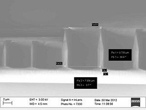
 Process date: February 2012 bghe@nanolab Recipe: m_poly@60degrees Process time: 25 min Mask: Poly Si 1.8 µm Etch depth: 12.5 µm Line width mask: 6µm Line with after etch: 3.4µm |
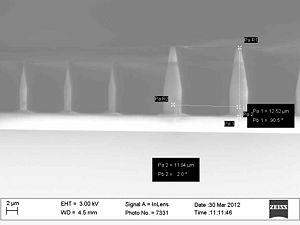
 Process date: February 2012 bghe@nanolab Recipe: m_poly@60degrees Process time: 25 min Mask: Poly Si 1.8 µm Etch depth: 12.5 µm Line width mask: 4µm Line with after etch: 1.5µm Sharp tip/edge is formed because the Si mask is completely etched away man the line becomes lower that the wider lines due to this. |
