| 29/11-2019
|
Medusa One
|
Si / 10%
|
stab-19 chamber clean 20
|
nanolab/ jmli /DREM 3.0 kW 100% b
|
S018653
|
Process log entry
|
|
|
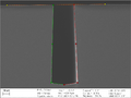
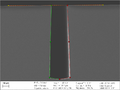
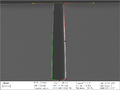
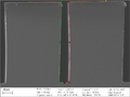
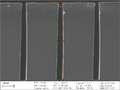
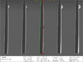
| SEM image:
|
a000
|
a001
|
a002
|
a003
|
a004
|
a005
|
a006
|
a007
|
a008
|
a009
|
a010
|
a011
|
a012
|
a013
|
| Trench width (um) |
159.77 |
401.82 |
251.88 |
250.36 |
158.96 |
99.72 |
61.82 |
40.77 |
32.13 |
25.67 |
12.84 |
7.24 |
4.13 |
2.6
|
| Etched depth (um) |
145.56 |
145.42 |
145.8 |
147.62 |
146.52 |
142.74 |
136.64 |
128.65 |
123.88 |
118.18 |
100.34 |
84.65 |
69.04 |
60.36
|
| Etch rate (um/min) |
14.56 |
14.54 |
14.58 |
14.76 |
14.65 |
14.27 |
13.66 |
12.86 |
12.39 |
11.82 |
10.03 |
8.46 |
6.9 |
6.04
|
| Etch rate (nm/cyc) |
1.21 |
1.21 |
1.21 |
1.23 |
1.22 |
1.19 |
1.14 |
1.07 |
1.03 |
0.98 |
0.84 |
0.71 |
0.58 |
0.5
|
| Sidewall bowing (%) |
-0.28 |
-0.51 |
-0.38 |
-0.38 |
-0.4 |
0.05 |
0.18 |
-0.14 |
0.09 |
0.19 |
0.36 |
0.45 |
0.52 |
0.53
|
| Sidewall angle (degs) |
92.65 |
93.1 |
92.66 |
93.02 |
92.84 |
92.17 |
92.04 |
91.86 |
91.92 |
91.7 |
91.52 |
91.05 |
90.71 |
90.61
|
| Bottom bowing (%) |
8.1 |
3.9 |
6.18 |
6.71 |
9.14 |
10.53 |
14.26 |
17.43 |
16 |
16.76 |
15.69 |
16.18 |
14.53 |
11.69
|
| Aspect ratio |
0.87 |
0.35 |
0.56 |
0.57 |
0.88 |
1.36 |
2.05 |
2.86 |
3.41 |
4.05 |
6.47 |
9.64 |
13.86 |
18.56
|
|


