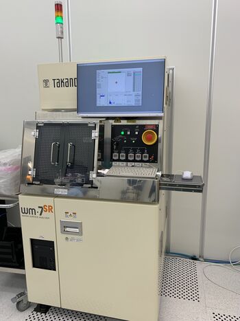
Specific Process Knowledge/Characterization/Particle Scanner Takano
Takano WM-7SR Wafer Surface Analyzer
Unless otherwise stated, this page is written by Patama Pholprasit DTU Nanolab internal
The Takano WM-7SR wafer surface analyzer is being used to analyze unpatterned surfaces on wafers for particles. The instrument detects, counts and sizes defects on wafers with semiconductor substrate materials. The instrument uses a 405 nm laser beam which is scanning over the wafer surface to detect defect contamination, i.e. particles. When the laser beam hits a particle, it will scatter and be detected. The scan results are displayed in color-coded wafer maps, histograms and summaries.

Specifications
- Particles having a size between 79 nm um and 5 um can be detected. The minimum particle size can only be detected on smooth surfaces such as bare silicon wafers or wafers with thermal SiO2.
- The detected particles sizes depends on the used gain setting.
- Wafer cassettes are available for 4”, 6” and 8” wafers. For the 4” wafer cassette, an adapter has to be mounted on the indexer.
- The wafer thickness should be a standard wafer thickness +/- 200 nm. Wafers that thicker than 1 mm need to get an approval from a responsible person.
- Area Count software function which helps to detect the larger particles (>11um) is not currently equipped but it is available for purchase.
The user manual, technical information and contact information can be found in LabManager:
