Specific Process Knowledge/Thin film deposition/Deposition of Nickel/Electroplating of nickel
Electroplating of nickel: Danchip standard processes
Feedback to this page: click here
DTU Danchip Standard Programs
Four different Danchip standard programs have been made. They have all been made to fabricate nickel shims for use in the polymer injection molder at Danchip. For this purpose a nickel thickness of around 320-330 µm is required. By experimentation it has been found that the required charge for this sample thickness is 18,0 Ah. The only difference between the four different standard programs are the time required for depositing the nickel. The four different standard programs deposit 320-330 µm of nickel in about 3, 4, 6 and 12 hours respectively.
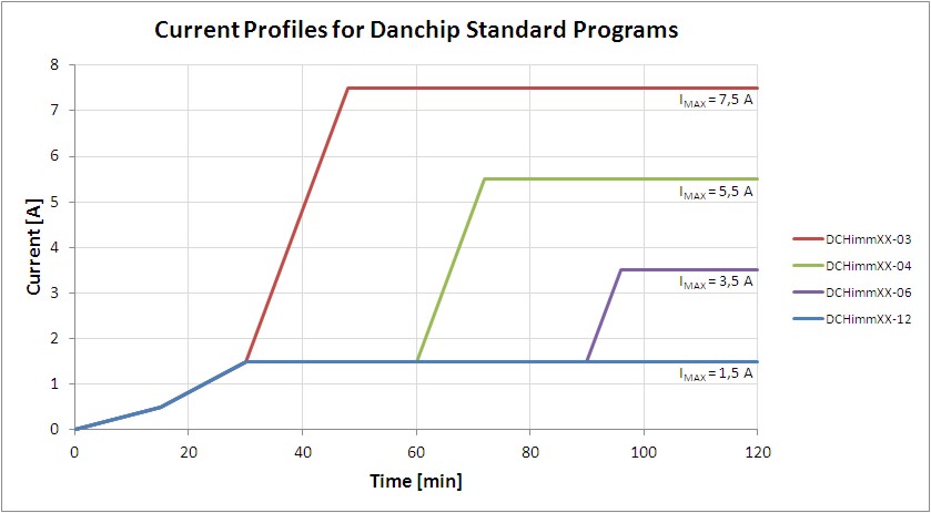
The following figure shows the current profile during the first 2 hours of the programs:

As can be seen from the illustration the first 30 minutes of all standard processes are identical. All processes use a slow ramping of the current. This is to make sure that some material is deposited which can conduct a higher current. Starting a plating process at several amperes is very likely to damage the sample (and possibly the sample holder) because the seed layer (usually 75-120 nm thick) cannot support that high current.
Comparison of standard processes
| DCHimm18-03 | DCHimm18-04 | DCHimm18-06 | DCHimm18-12 | |
|---|---|---|---|---|
| Expected nickel thickness | 320-330 µm | 320-330 µm | 320-330 µm | 320-330 µm |
| Maximum current [A] |
7,5 |
5,5 |
3,5 |
1,5 |
| Process time [hh:mm:ss] |
02:41:01 |
xx:xx:xx |
xx:xx:xx |
12:16:01 |
| Substrate size |
|
| ||
| Allowed materials |
|
|
Example
Feedback to this page: click here
Deposition of silicon nitride
Deposition of silicon nitride can be done with either LPCVD (Low Pressure Chemical Vapor Deposition) or PECVD (Plasma Enhanced Chemical Vapor Deposition). Stiochiometric nitride or silicon rich (low stress) LPCVD nitride is deposited on a batch of wafers in a LPCVD nitride furnace, and PECVD nitride (or oxynitride) is deposited on a few samples at a time in a PECVD system. LPCVD nitride has a good step coverage and a very good uniformity. Using PECVD it is possible to deposit a thicker layer of nitride on different types of samples, but the nitride does not cover sidewalls very well.
- Nitride deposition using PECVD (or oxynitride)
Comparison of LPCVD and PECVD for silicon nitride deposition
| LPCVD | PECVD | |
|---|---|---|
| Generel description | Low Pressure Chemical Vapour Deposition (LPCVD furnace process) | Plasma Enhanced Chemical Vapour Deposition (PECVD process) |
| Stoichiometry |
Si3N4: Stoichiometric nitride SRN: Silicon rich (low stress) nitride |
Silicon nitride can be doped with boron, phosphorus or germanium |
| Film thickness |
Thicker nitride layers can be deposited over more runs |
|
| Process temperature |
|
|
| Step coverage |
|
|
| Film quality |
|
|
| KOH etch rate (80 oC) |
|
|
| BHF etch rate |
|
|
| Batch size |
Depending on what furnace you use |
Depending on what PECVD you use |
| Allowed materials |
Processed wafers have to be RCA cleaned |
|
