Specific Process Knowledge/Etch/Etching of Silicon/Si etch using RIE1 or RIE2/Specific Process Knowledge/Etch/Etching of Silicon/Si etch using RIE1 or RIE2/RIE1 Travka results
THIS PAGE IS UNDER CONSTRUCTION

RIE1 Travka results - Silicon etch rate and profile as function of etch load
Purpose
The purpose of the RIE1 Travka experiments is to measure the silicon etch rate and profile as function of the etch load, i.e. of the percentage of the wafer that is etched.
Experiment
Seven silicon wafers have been etched in RIE1 using the "OH_polyA" recipe. The wafers have been etched in June 2012.
All wafers have the same resist pattern ("Travka" masks), but the etch load differs from wafer to wafer. A description of the process flow is show in the table below. For more information about the "Travka" masks see Travka masks.
Measurements
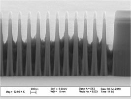
After the etching the wafers have been cleaved, and trechnes with different mask widths have been inspected with SEM in order to measure resist etch rate, the Si etch depth, the underetch and the trench width. From the Si etch depth the Si etch rate has been calculated.
The resist thickness has been measured on the Filmtek before and after the RIE etching, and thus the resist etch rate is calculted.
Process flow and parameters
| Photolithography | Resist thickness |
|
|---|---|---|
| Resist masks and etch loads |
| |
| Measure resist thickness | Filmtek parameters |
|
| RIE preconditioning | Before preconditioning |
|
| RIE1 preconditioning parameters |
| |
| RIE etching | Before etching |
|
| RIE1 etching parameters |
| |
| Note |
| |
| Measure resist thickness | Filmtek parameters |
|
| SEM characterization | Note |
|
| Mask trench widths to be measured |
| |
| Measurements |
|
Results
Silicon etch rate as function
- Result of InP etching. David Larsson, DTU Photonics, 2011


A table with the etching result can be found here:
xxx
| Mask | Resist etch rate [nm/min] | Silicon etch rate [µm/min] | Trench width [µm] | Under etch [µm] | Silicon etch angle [oC] | ||||||||||||||||||
|---|---|---|---|---|---|---|---|---|---|---|---|---|---|---|---|---|---|---|---|---|---|---|---|
| 2 µm | 4 µm | 10 µm | 50 µm | 200 µm | 2 µm | 4 µm | 10 µm | 50 µm | 200 µm | 2 µm | 4 µm | 10 µm | 50 µm | 200 µm | 2 µm | 4 µm | 10 µm | 50 µm | 200 µm | ||||
| Travka5 | 67.31 | 0.6 | 0.63 | 0.63 | 0.62 | 0.61 | 2.60 | 4,91 | 10.96 | 51.00 | 201.90 | ||||||||||||
| Travka10 | 63.94 | 0.57 | 0.59 | 0.59 | 0.58 | 0.61 | 2.32 | 4.60 | |||||||||||||||
| Travka20 | 63.13 | 0.63 | 0.63 | 0.64 | 0.64 | 0.59 | |||||||||||||||||
| Travka35 | 59.63 | 0.57 | 0.60 | 0.61 | 0.61 | 0.55 | |||||||||||||||||
| Travka50 | 57.13 | 0.47 | 0.5 | 0.51 | 0.51 | 0.49 | |||||||||||||||||
| Travka65 | 57.88 | 0.41 | 0.41 | 0.42 | 0.42 | 0.43 | |||||||||||||||||
| Travka80 | 57.56 | 0.37 | 0.36 | 0.37 | 0.37 | 0.38 | |||||||||||||||||
| Common | Temperature 20 degs, HBC 10 torr, Short funnel, with baffle & 5mm spacers | ||||||||||||||||||||||