Specific Process Knowledge/Thin film deposition/ALD Picosun R200/Al2O3 deposition using ALD
Feedback to this page: click here
This page is written by Evgeniy Shkondin @DTU Nanolab if nothing else is stated.
All images and photos on this page belongs to DTU Nanolab.
The fabrication and characterization described below were conducted in 2022 by Evgeniy Shkondin, DTU Nanolab.
Deposition of Al2O3 is a standard, and probably the most explored ALD process. In any book where ALD is explained or scientific reviews on a subject, the Al2O3 process is mentioned as a standard example with the corresponding reaction mechanism. In any facility where you find an ALD tool, you will also find an Al2O3 process since the film is very popular in many applications due to the ease of deposition, excellent uniformity, strict thickness control, and reliability. At DTU Naolab you can either use ALD-1 or ALD-2 for the deposition of Al2O3 with thermal (ALD-1 or ALD-2) or plasma (ALD-2) methods.
Al2O3 ALD deposition using TMA and H2O
Al2O3 can be deposited in the range between 100 °C to 300 °C. It is not recommended to increase the temperature above 300 °C, due to the decomposition of TMA. The maximum temperature can be 350 °C, here however the deposition rate will decrease and the film will most likely contain a minor amount of Al clusters incorporation.
Al2O3O recipes
Recipe: Al2O3
Maximum deposition thickness: 100 nm
Temperature: 100 °C - 300 °C
| TMA* | H2O | |
|---|---|---|
| Nitrogen flow | 150 sccm | 200 sccm |
| Pulse time | 0.1 s | 0.1 s |
| Purge time | 3.0 s | 4.0 s |
This is a standard recipe of Al2O3. It is suitable for coating the flat samples and structures with an aspect ratio of around up to 1:10.
Recipe: Al2O3T
Maximum deposition thickness: 100 nm
Temperature: 100 °C - 300 °C
| TMA* | TMA | H2O | H2O | |
|---|---|---|---|---|
| Nitrogen flow | 150 sccm | 150 sccm | 200 sccm | 200 sccm |
| Pulse time | 0.1 s | 0.1 s | 0.1 s | 0.1 s |
| Purge time | 0.5 s | 20.0 s | 0.5 s | 20.0 s |
This is a more complicated recipe that allows coating the sample with very high aspect ratio profiles. The recipe is good for deposition on very high aspect ratio structures (with aspect ratio more than 1:20) such as deep trenches, pillars, pores etc. Al2O3T recipe can also be used for deposition on polymers at low temperatures (80-120 °C).
TMA is trimethylaluminium: Al(CH3)3
Deposition characteristics
The deposition rate for Al2O3 depends on the temperature, see the ALD-window graph below. The uniformity, thickness, refractive index has been obtained using Ellipsometer VASE.
Deposition rate
-
 Deposition rate of Al2O3 at 100 °C. Substrate: Silicon 4" wafer with native oxide.
-
 Deposition rate of Al2O3 at 150 °C. Substrate: Silicon 4" wafer with native oxide.
-
 Deposition rate of Al2O3 at 200 °C. Substrate: Silicon 4" wafer with native oxide.
-
 Deposition rate of Al2O3 at 250 °C. Substrate: Silicon 4" wafer with native oxide.
-
 Deposition rate of Al2O3 at 300 °C. Substrate: Silicon 4" wafer with native oxide.
-
 Deposition rate of Al2O3 at 350 °C. Substrate: Silicon 4" wafer with native oxide.
-
 ALD window of Al2O3


Uniformity across 100 mm wafer
Recipe "Al2O3" Samples: 100mm ssp-Si
Results have been obtained for <100> 100 mm Si wafers with native oxide, based on ellipsometry study.
| Temperature (°C) / Number of cycles | Deposition rate (nm/s) | Average thickness (nm) | Standard deviation | Uniformity (%) |
|---|---|---|---|---|
| 100°C / 500cycles | 0.0928 | 46.20 | 0.47 | 1.98 |
| 150°C / 500cycles | 0.1026 | 51.22 | 0.50 | 1.83 |
| 200°C / 500cycles | 0.1064 | 53.42 | 0.52 | 1.76 |
| 250°C / 500cycles | 0.1056 | 53.16 | 0.29 | 0.99 |
| 300°C / 500cycles | 0.0990 | 49.29 | 0.19 | 0.66 |
| 350°C / 500cycles | 0.0895 | 44.83 | 0.20 | 0.76 |
-
 Uniformity across 100mm wafer. Deposition at 100°C
 -
 Uniformity across 100mm wafer. Deposition at 150°C
 -
 Uniformity across 100mm wafer. Deposition at 200°C
 -
 Uniformity across 100mm wafer. Deposition at 250°C
 -
 Uniformity across 100mm wafer. Deposition at 300°C
 -
 Uniformity across 100mm wafer. Deposition at 350°C


Optical functions
Results have been obtained for <100> 100 mm Si wafers with native oxide, based on ellipsometry study. Cauchy model has been implemented for refractive index fitting.
-
 Refractive index of 50 nm Al2O3 deposited on silicon at different temperatures.
 -
 Optical transmission of 100 nm Al2O3 deposited on fused silica wafer at 200C.


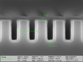
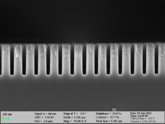
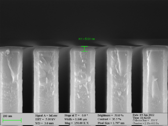
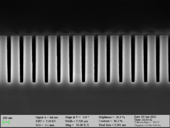
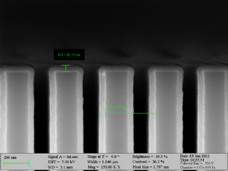
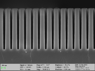
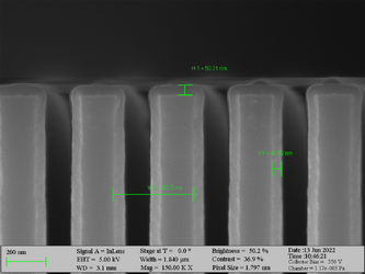
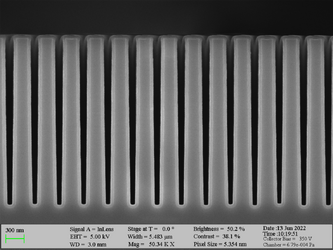
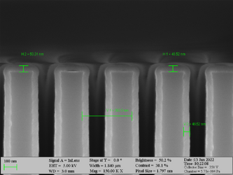
Deposition on high aspect ratio structures (SEM inspection)
Aluminum oxide has been deposited on Si trench structures to see the uniformity of the layer. The standard recipe “Al2O3” was implemented. The trenches were inspected using SEM in cross-sectional mode.
-
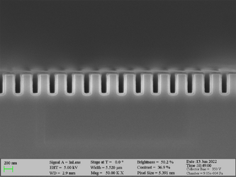 Deposition of Al2O3 on high aspect ratio Si trench structures. The trench height is 500 nm. Deposition conditions: 100°C and 500 cycles. A Standard “Al2O3” recipe was used.
 -
 Deposition of Al2O3 on high aspect ratio Si trench structures. The trench height is 500 nm. Deposition conditions: 100°C and 500 cycles. A Standard “Al2O3” recipe was used.
 -
 Deposition of Al2O3 on high aspect ratio Si trench structures. The trench height is 1000 nm. Deposition conditions: 100°C and 500 cycles. A Standard “Al2O3” recipe was used.
 -
 Deposition of Al2O3 on high aspect ratio Si trench structures. The trench height is 1000 nm. Deposition conditions: 100°C and 500 cycles. A Standard “Al2O3” recipe was used.
 -
 Deposition of Al2O3 on high aspect ratio Si trench structures. The trench height is 1500 nm. Deposition conditions: 100°C and 500 cycles. A Standard “Al2O3” recipe was used.
 -
 Deposition of Al2O3 on high aspect ratio Si trench structures. The trench height is 1500 nm. Deposition conditions: 100°C and 500 cycles. A Standard “Al2O3” recipe was used.
 -
 Deposition of Al2O3 on high aspect ratio Si trench structures. The trench height is 2000 nm. Deposition conditions: 100°C and 500 cycles. A Standard “Al2O3” recipe was used.
 -
 Deposition of Al2O3 on high aspect ratio Si trench structures. The trench height is 2000 nm. Deposition conditions: 100°C and 500 cycles. A Standard “Al2O3” recipe was used.
 -
 Deposition of Al2O3 on high aspect ratio Si trench structures. The trench height is 2500 nm. Deposition conditions: 100°C and 500 cycles. A Standard “Al2O3” recipe was used.
 -
 Deposition of Al2O3 on high aspect ratio Si trench structures. The trench height is 2500 nm. Deposition conditions: 100°C and 500 cycles. A Standard “Al2O3” recipe was used.
 -
 Deposition of Al2O3 on high aspect ratio Si trench structures. The trench height is 3000 nm. Deposition conditions: 100°C and 500 cycles. A Standard “Al2O3” recipe was used.
 -
 Deposition of Al2O3 on high aspect ratio Si trench structures. The trench height is 3000 nm. Deposition conditions: 100°C and 500 cycles. A Standard “Al2O3” recipe was used.


X-ray photoelectron spectroscopy
XPS measurements of all samples has been performed using the XPS NEXSA equipment. The purpose of the investigation is to get an idea about the film stoichiometry, composition and possible contamination. Since the XPS NEXSA also offers REELS and ISS analysis these measurements were also performed.
The XPS Nexsa is equipped with the MAGCIS or Mono Atomic and Gas Cluster Ion Source that allows to sputter off material from the sample either using single argon atoms with energies up to 4 keV or by using ionized clusters of argon atoms (between 75 and 2000 atoms) with energies up to 8 keV. For this analysis, the native carbon contamination has been removed by Ar clusters at 4keV and a size of 300 atoms. The moisture level has been sputtered off by implementing 25 levels at 5 s each.
- MAGCIS cleaning of Al2O3 film surface
-
 Removal of native carbon by Ar clusters.
 -
 Removal of native carbon by Ar clusters. 2D profile.


After the surface has been cleaned, the film has been measured, so the survey, valence region, and high-resolution elements (Al, O, and C) scan have been acquired.
-
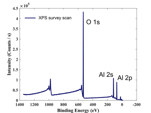 Survey scan after removal of the native carbon.
 -
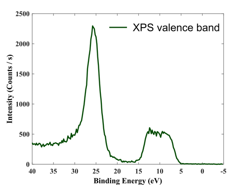 Valence region.


-
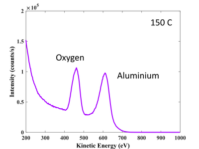
 Al 2p signal. High resolution scan. 100°C.
 -
 Al 2p signal. High resolution scan. 150°C.
 -
 Al 2p signal. High resolution scan. 200°C.
 -
 Al 2p signal. High resolution scan. 250°C.
 -
 Al 2p signal. High resolution scan. 300°C.
 -
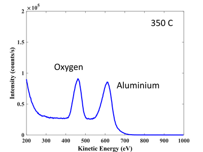
 Al 2p signal. High resolution scan. 350°C.
 -
 O 1s signal. High resolution scan. 100°C.
 -
 O 1s signal. High resolution scan. 150°C.
 -
 O 1s signal. High resolution scan. 200°C.
 -
 O 1s signal. High resolution scan. 250°C.
 -
 O 1s signal. High resolution scan. 300°C.
 -
 O 1s signal. High resolution scan. 350°C.


Stoichiometry results
No traces of carbon has been found.
| Stoichiometry results for Al2O3 deposited with TMA and H2O. | ||||||
|---|---|---|---|---|---|---|
| Temperature °C | 100 | 150 | 200 | 250 | 300 | 350 |
| Number of cycles | 500 | 500 | 500 | 500 | 500 | 500 |
| Al (At. %) | 60.53 | 45.61 | 39.03 | 39.20 | 39.36 | 38.98 |
| O (At. %) | 39.47 | 54.39 | 60.97 | 60.20 | 60.64 | 61.02 |
REELS and ISS
Reflected Electron Energy Loss Spectroscopy (REELS) involves the exposure of the sample to a focused beam of monoenergetic electrons at 1keV coming from the flood gun. As these electrons interact with the material some of them will undergo inelastic scattering whereby they lose some kinetic energy. In reflection electron energy loss (REELS) the electrons that are both elastically and inelastically scattered are collected using the electron energy analyzer. The low-energy electron energy loss spectrum (up to ~50eV in energy loss) contains the elastic, or zero-loss, peak as well as the plasmon peaks. This spectrum can be used to determine information about the band structure and dielectric properties of the sample.
Calculated sampling depth for a 1 keV REELS experiment is ca. 15 nm, although it is noted that this will be dependent on the material being analyzed. Information from the REEL spectrum is complementary to other surface sensitive techniques, including XPS.
Ion scattering spectroscopy (ISS) is a technique in which a beam of He+ ions is scattered by a surface. The kinetic energy of scattered ions is measured; peaks are observed corresponding to elastic scattering of ions from atoms at the surface of the sample. Each element at the sample surface produces a peak at a different measured kinetic energy, caused by the momentum transfer between the incident ion and atom. The scattered ion and the scattering atom are normally of different masses, but the total momentum of the atom and ion is conserved. Therefore, as the initially "stationary" atom recoils, some kinetic energy is lost from the scattered ion, and the quantity of lost energy depends on the relative masses of the atom and ion. An ion scattering spectrum typically contains one peak for each element in the sample, with their separation in energy relating to the relative atomic masses of those elements. In some cases, different isotopes of the same element can be resolved, although this usually requires a primary ion heavier than He+. Strong scattering signals are limited to the topmost layer of atoms, so ISS is extremely surface-sensitive. Therefore, the sample must be clean, and even a small quantity of surface contaminant can significantly influence the ion scattering spectrum. Find more information here: https://www.thermofisher.com/dk/en/home/materials-science/learning-center/surface-analysis.html
ISS
-
 ISS spectrum. (low current, Beam energy: 1kEv)
 -
 ISS spectrum. (low current, Beam energy: 1kEv)
 -
 ISS spectrum. (low current, Beam energy: 1kEv)
 -
 ISS spectrum. (low current, Beam energy: 1kEv)
 -
 ISS spectrum. (low current, Beam energy: 1kEv)
 -
 ISS spectrum. (low current, Beam energy: 1kEv)
 -
 ISS spectrum. (low current, Beam energy: 1kEv)


REELS
-
 REELS spectrum
-
 REELS spectrum
-
 REELS spectrum
-
 REELS spectrum
-
 REELS spectrum
-
 REELS spectrum


X-ray reflectivity analysis
X-ray reflectivity analysis (XRR) of two samples (100 nm film deposited at 200°C and 35 nm film deposited at 3000°C) have been performed to investigate the thicknesses, roughness, and density profiles.
The scans have been obtained using Rigaku XRD SmartLab equipment. The voltage and current settings for the Cu X-ray tube were standard 40kV and 30mA. The incident optics contained an IPS (incident parallel slit) adaptor with 5 ° Soller slit. Other slits: IS=0.03mm RS1=0.03mm and RS2=0.075mm. Step size: 0.01 and measurement time - 5s for each point. The fitting process was performed using commercial GlobalFit software assuming the model based on Si or SiO2 substrates with native oxide/interlayer followed by the deposited TiO2 film and moisture surfaces. The results are summarized in the tables below.
-
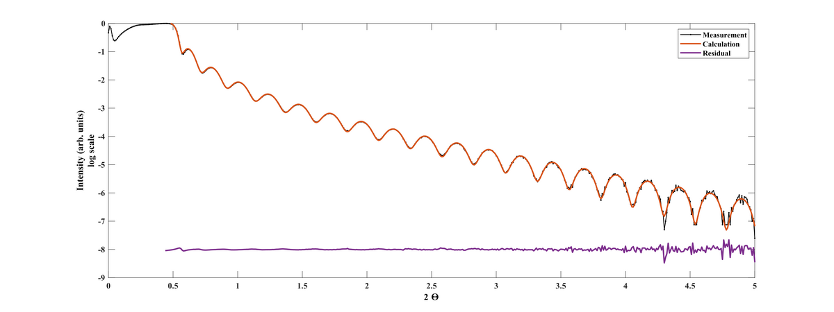 XRR scan of Al2O3 film deposited at 300°C and 350 cycles.
 -
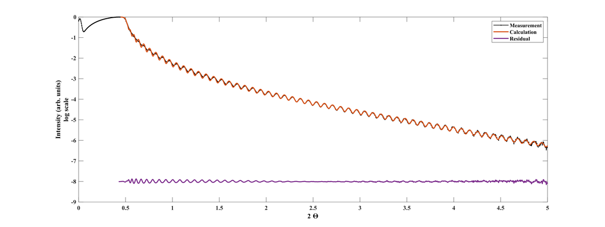 XRR scan of Al2O3 film deposited at 200°C and 930 cycles.


| XRR results for Al2O3 layers | |||||||||||||||||||||||||||||||||||||||||||||||||||||||||||||||||||||||||||||||||||||||||||||||||||||||||||||||||||||||||||||
| |||||||||||||||||||||||||||||||||||||||||||||||||||||||||||||||||||||||||||||||||||||||||||||||||||||||||||||||||||||||||||||