Specific Process Knowledge/Etch/Etching of Silicon Oxide/SiO2 etch using ASE/ICP recipe for SiO2

From LabAdviser
Jump to navigation Jump to search

This recipe was taken from the ICP Metal etch, with a slight difference in the platen temperature.
Material to be etched Recipe: 1SiO2_02 *This recipe is no longer stable. Recipe: 1SiO2_03 Testing other settings to increase etch rate in nitride
Etch rate in SiO2 22.1 nm/min 26.8 nm/min ?
Etch rate in PECVD nitride . 20.8nm/min (kabi@nanolab 20190301) - ~0nm/min (ecsj@nanolab 20210729) ?
Etch rate in LPCVD nitride . only around 6 nm/min (20190820) 23.7 nm/min in the middle, 17 nm/min close to the edge
Etch rate in resist (MIR) 12.5 nm/min 13.9 nm/min Not tested properly (still more than 1 µm left (1.5µm MIR) after 12 min
Selectivity (SiO2:resist) 1.8 1.9 ?
Etch rate in silicon
  • 4 nm/min in the middle of the wafer (80% load) bghe@Nanolab 20190117
  • 2-3 nm/min at the edge of the wafer (80% load) bghe@Nanolab 20190117
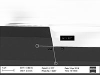
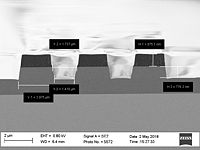
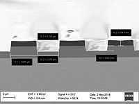
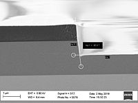
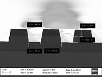
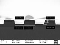
Profile Images SiO2ICP26 03.jpg SiO2ICP26 05.jpg SiO2ICP26 07.jpg SiO2ICP33 01.jpgSiO2ICP33 03.jpgSiO2ICP33 05.jpg Profile not analyzed