Specific Process Knowledge/Etch/Etching of Silicon Oxide/SiO2 etch using AOE/Standard recipe with resist mask/AOE SiO2 etch load dependency
Feedback to this page: click here
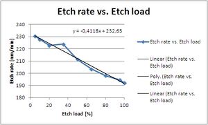
The etch rate dependency of the etch load
This page has been done by Berit Herstrøm @ DTU Nanolab (BGHE) if nothing else is stated
Etch load
Etch load is the percentage of the wafer surface that is exposed to the plasma. E.g. if you have a wafer with a surface of SiO2 where 95% of the surface is covered by photoresist (or another masking material that has a high selectivity to SiO2 with the used etcing recipe)the the etch load i 5%
Etch load effect of SiO2 etch with etch recipe SiO2_res and with photoresist as masking material
This work has been done by bghe@nanolab in February/Marts 2013
8 wafers with different etch load has been etched with the same recipe in the AOE: m_res_ny (now called SiO2_res 2019-06-26) for the same time and under that same conditions. This was done to isolate the etch load as a parameter to see how much that affects etch rate.
Samples
- 100mm SSP Si wafers 525µm in thickness
- 2.2 µm SiO2 grown in furnace: phospher drive-in, recipe Wet1100 for 10 hours
- 1.4 µm photoresist
- 5%-95% etch load - masks TRAVKA: 5%,10%,20%,35%,50%,65%,80% and 95%
AOE settings
Before each sample etch a 3 min TDESC clean was done to get the chamber in the same condition.
| Parameter | SiO2_res |
|---|---|
| Coil Power | 1300W |
| Platen Power | 200W |
| Platen temperature | 0oC |
| He flow | 174sccm |
| C4F8 flow | 5sccm |
| H2 flow | 4sccm |
| Pressure | 4mTorr |
| Etch time | 4min |
Results
| Ecth load: | 5% | 10% | 20% | 35% | 50% | 65% | 80% | 95% | Comment |
|---|---|---|---|---|---|---|---|---|---|
| Etch rate | 231±1.7nm/min | 228±1.5nm/min | 223±2.3nm/min | 224±2.7nm/min | 211±3.8nm/min | 203±4.6nm/min | 198±5.8nm/min | 192±5.1nm/min | "±" represents the non-uniformity over the wafer |
| Selectivity to resist 1: | 2.9 | 2.8 | 2.7 | 2.5 | 2.4 | 2.3 | 2.0 | 2.0 | |
| Non-uniformity over a 100mm wafer - 1cm exclusion zone | ±0.7% | ±0.7% | ±1.0% | ±1.2% | ±1.8% | ±2.3% | ±2.9% | ±2.7% |
Conclusion
- The etch rate decreases with etch load with aproximately 20%
- The wafer non-uniformity increases with etch load going from less than ±1% to about ±3%
- The selectivity to resist decreases with etch load from about 1:3 to about 1:2
