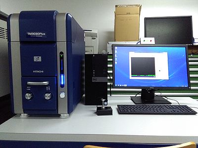
Specific Process Knowledge/Characterization/SEM Tabletop 1
Feedback to this page: click here

SEM Tabletop 1
The SEM Tabletop 1 is a scanning electron microscope. It produces enlarged images of a variety of specimens. This important and widely used analytical tool provides images with very good resolution and depth of field, and a minimal sample preparation is required.
The tabletop SEM has a thermionic filament made of tungsten.
The SEM chamber is relatively small, so sample loading can be done fast and easy.
The stage is moved manually in the X and Y directions by turning two knobs on the door to the SEM chamber. It is not possible to adjust the height of the stage, and it is not possible to rotate and tilt samples. However, samples can be mounted on pinstubs with a fixed tilt angle.
Many sample materials are allowed in the this SEM, including all standard cleanroom materials and samples from the Laser Micromachining tool and the Polymer Injection Molding tool. Some other materials, including biological materials, are also allowed if they have been approved by Nanolab.
It is not needed to perform much optimization in order to obtain good SEM images. However, the tabletop SEM has a limited resolution compared to the other SEMs at Nanolab, but for inspection of samples with structures in the micrometer range it is very fast and easy to use. It is not necessary to be an autorized user of the other SEMs at Nanolab to use the tabletop SEM.
The SEM can be operated in different pressure modes: Conductor, standard and charge-up reduction. By increasing the pressure in the chamber it is possible to inspect isolating samples, because the higher density of gas molecules will eliminate the charges at the cost of a slightly reduced resolution. Thus the charge-up reduction mode makes it possible to obtain SEM images of most samples including isolating samples without much sample preparation.
The SEM is equipped with two detectors: A secondary electron (SE) detector and a backscatter (BSE) detector.
The SEM Tabletop 1 was installed at DTU Nanolab in January 2017.
The user manual, control instruction, the user APV and contact information can be found in LabManager:
SEM Tabletop 1 info page in LabManager,
Performance information
Equipment performance
| Equipment | SEM Tabletop 1 (Hitachi TM3030 Plus ) | |
|---|---|---|
| Purpose | Imaging and measurement of |
|
| Location |
| |
| Performance | Resolution |
The resolution is strongly dependent on the type of sample and the skills of the operator. |
| Instrument specifics | Detectors |
|
| Stage |
| |
| Electron source |
| |
| Operating pressures |
| |
| Substrates | Sample size |
|
| Allowed materials |
| |
