Specific Process Knowledge/Thin film deposition/DiamondCVD
Feedback to this page: click here
THIS PAGE IS UNDER CONSTRUCTION
SEKI Diamond CVD
The SEKI AX5250S is a Microwave Plasma Chemical Vapor Deposition (MPCVD) system for growth of diamond thin films. The system is fitted with gases for diamond growth, which are hydrogen, methane, and oxygen.
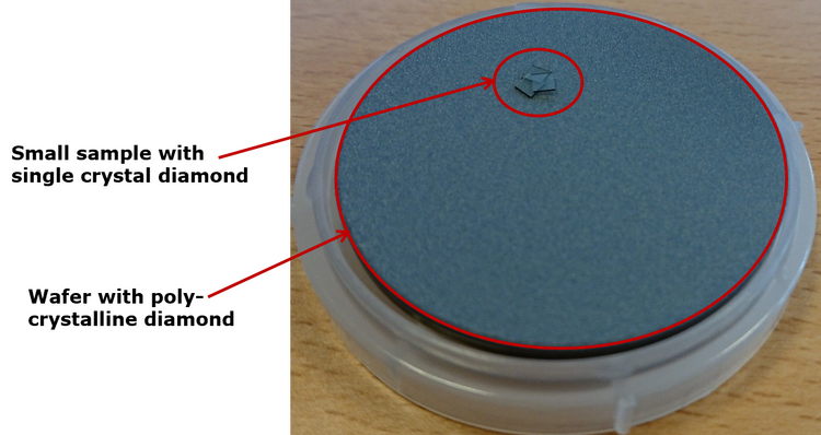
Depending on the starting material both polycrystalline and single crystalline diamond can be grown. Diamond has a lattice constant of 3.567 Å, which is not easily matched to other materials, and therefore in general diamond growth must be seeded by diamond as nucleation sites.
For single crystalline diamond this means that diamond layers in most cases must be grown on top of single crystal diamonds. For polycrystalline diamond, almost any material (which can handle 800 °C) will do. It just needs to be seeded with nano diamonds. The seeding can happen by immersion into solution, by polishing, or by spray coating with nano diamonds.
The user manual, APV, technical information, and contact information can be found in LabManager:
Diamond growth
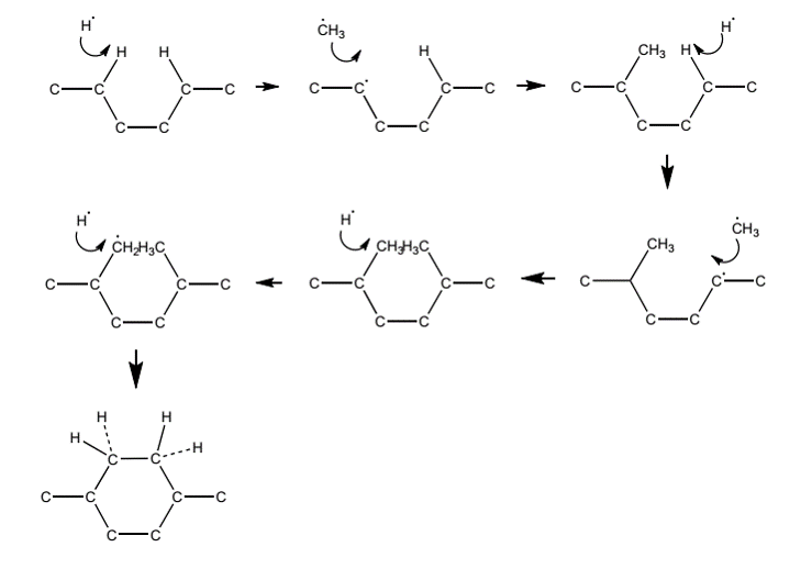
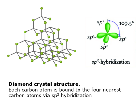
Diamond is grown by depositing carbon from the CH4 on a substrate. If the carbon forms an sp3 bond to other carbon atoms, diamond is grown. Otherwise it will be etched away by a high concentration of H2. Diamond is very inert, but the plasma in the CVD equipment creates hydrogen radicals that in turn create active sites on the diamond surface. These active sites react with methane radicals that are also created in the plasma.
Single- and polycrystalline diamond
It is possible to grow extremely clean diamond in the SEKI system. It is also possible to control the N2 dopant level and dopant depth. Nitrogen doping affects the optical and electronic properties of the diamond. For instance this can be used in magnetic sensors, which is a topic of research at DTU Physics.
For polycrystalline growth the substrate must be seeded with diamonds as mentioned above. This is commonly done by sonicating the substrate in a solution of water with nano diamonds. After sonication the substrate is rinsed in water and blow-dried.
Polishing is needed after deposition if the polycrystalline diamond layer has to be smooth. Thinning is needed if the diamond layer has to be very thin as a uniform diamond layer can only be deposited above 1 μm thickness.
| Equipment | SEKI AX5250S | |
|---|---|---|
| Purpose | Diamond growth |
|
| Parameters |
H2 |
1000 sccm |
|
CH4 |
50 sccm | |
|
O2 |
20 sccm | |
|
Operating pressure |
>200 Torr | |
|
Power |
5000 W | |
|
Temperature |
700-900 °C | |
| Process | Growth rate |
About 8 Å/s (3 μm/hr) |
| Max thickness |
About 100 μm | |
| Uniformity |
OK up to 50 mm diameter | |
| Substrates | Substrate size |
up to 100 mm wafers, 50 mm preferred |
| Allowed materials |
Ask | |


