Specific Process Knowledge/Thin film deposition/DiamondCVD
Feedback to this page: click here
THIS PAGE IS UNDER CONSTRUCTION
SEKI Diamond CVD
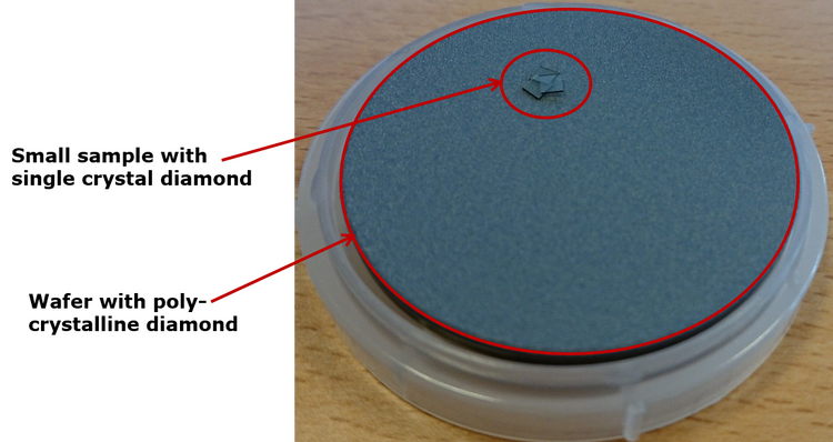
The SEKI AX5250S is a Microwave Plasma Chemical Vapor Deposition (MPCVD) system for growth of diamond thin films. The system is fitted with gases for diamond growth, which are hydrogen, methane, and oxygen. Depending on the starting material both polycrystalline and single crystalline diamond can be grown. Diamond has a lattice constant of 3.567 Å, which is not easily matched to other materials, and therefore in general diamond growth must be seeded by diamond as nucleation sites. For single crystalline diamond this means that diamond layers in most cases must be grown on top of single crystal diamonds. For polycrystalline diamond, almost any material (which can handle 800 °C) will do. It just needs to be seeded with nano diamonds. The seeding can happen by immersion into solution, by polishing, or by spray coating with nano diamonds.
The user manual, APV, technical information, and contact information can be found in LabManager:
Poly crystalline diamond growth
For polycrystalline growth, the substrate must be seeded with diamonds. This is commonly done by sonicating the substrate in a solution of water with nano diamonds. After sonication the substrate is rinsed in water and blow-dried.
| Equipment | SEKI AX5250S | |
|---|---|---|
| Purpose | Diamond growth |
|
| Parameters |
H2 |
1000 sccm |
|
CH4 |
50 sccm | |
|
O2 |
20 sccm | |
|
Operating pressure |
>200 Torr | |
|
Power |
5000 W | |
|
Temperature |
700-900 °C | |
| Substrates | Substrate size |
up to 100 mm wafers, 50 mm prefered |
| Allowed materials |
Ask | |


