LabAdviser/Technology Research/Nanofabrication of Inductive Components for Integrated Power Supply On Chip/3D Passive Interposer
One of the advantages of the TSV inductors is related to the possibility of fabrication of novel 3D passive interposers for co-packaged PSiP. The interposer includes two parts: a TSV air-core toroidal inductor and a interconnection part with extra TSVs and top/bottom Cu pads. The additional TSVs, which are used as vertical conductors for the in-silicon inductor, are designed to provide electrical connections through the Si wafer thus allowing co-packaged assembly of other active and passive components needed for power supplies. Furthermore, this approach can be developed towards the ultimate integration of PwrSoC using active interposers in which active components and passive inductors are all integrated on the same substrate.
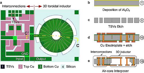
The designs of four photolithography masks are shown in Figure 3.25a. Mask 1 is for through-wafer Si etching to define the TSVs. Mask 2 and 3 are for Cu wet-etching to define the inductor windings. Mask 4 is for ICP Si-core etching in which the Si-core is removed while protecting the Si die and Si fixtures. The process is summarized in four steps which correspond to step 1, 5, 10, and 15 in Figure 3.3. The process starts with a preparation step (Figure 3.25b) of depositing 50 nm Al2O3 which is used as a hard masking material for through-wafer etching. The Si wafer is then etched through to create hollow TSVs (3.25c). A 50-µm Cu layer is firstly electroplated on the top surface to close the TSVs, the TSVs are then filled with Cu using bottom-up electroplating technique. A 50-µm Cu layer is then electroplated on the bottom surface. Photolithography is performed on both wafer sides to pattern the toroidal windings followed by a Cu wet-etching step (Figure 3.25d). The last step is to remove the Si-core using ICP isotropic Si etching. As shown in Figure 3.25e, only the Si in the toroidal core (right) is removed while the Si substrate on the left is protected.
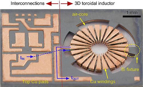
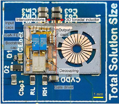
The 3D passive interposer was successfully fabricated on a 280-µm Si wafer and is shown in Figure 3.26. The interposer consists of two parts including an interconnection part (left) and a 3D TSV air-core toroidal inductor (right). The toroidal inductor has a size of 1.8 x 1.8 x 0.28 mm, 25 turns and 50-µm-diameter TSVs. There are two parallel inner TSVs and four parallel outer TSVs. This inductor is designed to have 50 nH inductance. As shown in the interconnection part, the 50-µm-thick top Cu pads, which are fabricated by Cu wet etching, are used to assemble a half-bridge buck converter using two 40 V GaN FETs (EPC8004), a gate driver (PE29100), and capacitors. The layout is designed to match the component's layout. The bottom Cu pads provides connections to the underlying main PCB via TSVs.
(a) A layout design of a 3D passive interposer with 4 layers including TSVs, top copper, bottom copper, and silicon. The interposer consists of a 3D toroidal inductor and a interposer part with additional TSVs and top/bottom copper pads as shown in Figure 3.25d, e. The fabrication process of the interposer is similar to the fabrication process for the TSV air-core toroidal inductor (Figure 3.3). Fabrication process ow for 3D passive interposer is presented in C-C' direction. There are four mains steps: including: (b) a preparation step with the deposition of ALD Al2O3 layer on a 4-inch Si wafer, (c) through-wafer DRIE Si etch to create TSVs, (d) copper electroplating and wet etching, (e) Si-core removal using ICP Si etch and releasing steps.
Fabrication results of 3D passive interposers. A micrograph of a passive interposer with an embedded 3D TSV air-core toroidal inductor (right) and the interconnection part (left) with TSVs and top and bottom Cu pads for PSiP assembly. The inductor has 25 turns and freestanding Cu windings secured by 5 Si fixtures. The inductor's input and output are connected to the switching node and the converter output, respectively, as depicted by the blue arrows.
The assembly process to implement the fabricated interposer on a power supply is carefully developed with an extra attention on the procedure of components assembling
and reflowing. To avoid misalignment due to multiple reflowing steps, two solver pastes with two
melting temperatures 215 oC (paste 1) and 180 oC (paste 2). The solder pastes were dispensed under
a microscope using 0.2-mm-diameter needles at a pressure of 7 bar.There are three steps in the assembly procedure: (i) dispense the high-temperature paste 1 on a main PCB using a fine needle, align and mount the fabricated passive interposer, and reflow the sample using a temperature profile of 175 oC
for 5 minutes and 230 oC for 3 minutes. (ii) dispense a low-temperature paste 2 on the top Cu pads of the
passive interposer, align and mount the components, and reflow at 200 oC for 3 minutes. (iii) assemble
the remaining components on the main PCB and reflow.
An assembled power stage on an interposer with two GaN FETs, a gate driver, and capacitors.
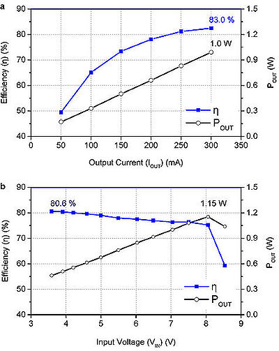
Measured eficiency and output power with (a) Output current from 50 mA to 300 mA, (b) Input voltage from 3.5 V to 8.5 V with an output voltage of 3.3 V.


